MX63 / MX63L


Overview
Streamline Your Large Sample Inspection Workflow
The MX63 and MX63L microscope systems are optimized for high-quality inspections of wafers as large as 300 mm, flat panel displays, circuit boards, and other large samples. Their modular design enables you to choose the components you need to tailor the system to your application.
These ergonomic and user-friendly microscopes help increase throughput while keeping inspectors comfortable while they do their work. Combined with PRECiV image analysis software, your entire workflow, from observation to report creation, can be simplified.

Functional
Designed to meet the ergonomic and safety requirements of the electronics industry with added functionality to enhance analysis capabilities.
User-Friendly
Simplified microscope settings makes it easier for users to make adjustments and reproduce system settings.
Advanced Imaging Technology
Our proven optics and exceptional imaging technology deliver clear images and reliable inspections.
Modular
Users can customize their system with the components that suit their application.
Application Image Gallery
Our advanced image management capability shows what you really want to observe.
Functionality
Observation and Analysis Tools
Leading-Edge Analysis Tools
The MX63 series’ versatile observation capabilities provide clear, sharp images so users can reliably detect defects in their samples. New illumination techniques and image acquisition options within PRECiV image analysis software give users more choices for evaluating their samples and documenting their findings.
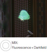
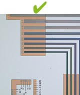
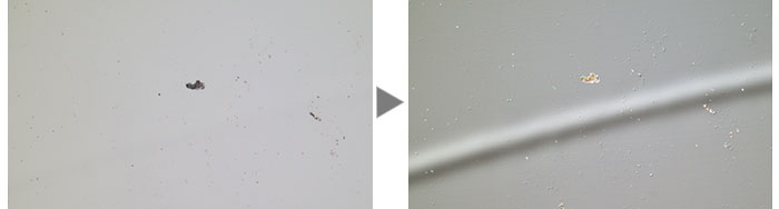
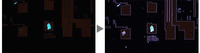
The Invisible Becomes Visible: MIX Observation and acquisition
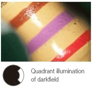
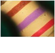
MIX observation technology produces unique observation images by combining darkfield with another observation method, such as brightfield, fluorescence, or polarization. MIX observation enables users to view defects that are difficult to see with conventional microscopes. The circular LED illuminator used for darkfield observation has a directional darkfield function where only one quadrant is illuminated at a given time. This reduces a sample’s halation and is useful for visualizing a sample’s surface texture.
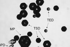
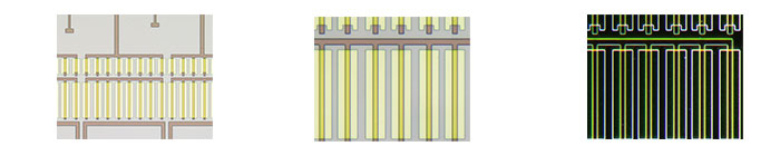
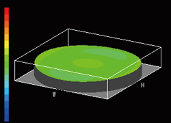
Structure on semiconductor wafer
|
|
|
|
| ||
The IC pattern is unclear. | The wafer color is invisible. | Both the wafer color and IC pattern are clearly represented. |


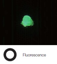
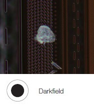
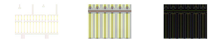
Photoresist residue on a semiconductor wafer
|
|
|
|
| ||
The sample itself is invisible. | The residue is unclear. | Both the IC pattern and residue are clearly represented. |
Condenser
|
|
|
|
| ||
The surface is reflected. | Several images with directional darkfield from different angles. | By stitching together clear images with no halation, a single crisp image of the sample is created. |

Easily Create Panoramic Images: Instant MIA
With multiple image alignment (MIA), users can stitch images together quickly and easily simply by moving the KY knobs on the manual stage—a motorized stage is not necessary. PRECiV software uses pattern recognition to generate a panoramic image, giving users a wider field of view.
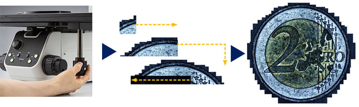
Instant MIA image of a coin
Create all-in-focus images: EFI
The Extended Focus Imaging (EFI) function within PRECiV captures images of samples whose height extends beyond the depth of focus of the objective and stacks them together to create one image that is all in focus. EFI can be executed with either a manual or motorized Z-axis and creates a height map for easy structure visualization. It is also possible to construct an EFI image while offline within Stream Desktop.
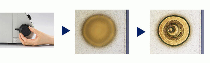
Stud bump on an IC chip
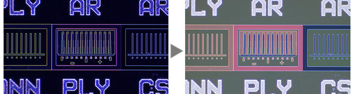
Capture Both Bright and Dark Areas Using HDR
Using advanced image processing, high dynamic range (HDR) adjusts for differences in brightness within an image to reduce glare. HDR improves the visual quality of digital images thereby helping to generate professional-looking reports.
|
|
|
|
|
| |||
Some areas are glaring. | Both dark and bright areas are clearly exposed by HDR. | The TFT array is blacked out due to the brightness of the color filter. | The TFT array is exposed by HDR. |


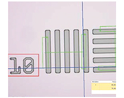
From Basic Measurement to Advanced Analysis
Measurement is essential to quality and process control and inspection. With this in mind, even the entry-level PRECiV software package includes a full menu of interactive measurement functions, with all measurement results saved with image files for further documentation. In addition, the PRECiV Materials Solution offers an intuitive, workflow-oriented interface for complex image analysis. At the click of a button, image analysis tasks can be executed quickly and precisely. With a significant reduction in processing time for repeated tasks, operators can concentrate on the inspection at hand.
Basic measurement (pattern on a printed circuit board) |
Throwing power solution (Cross section of a through hole of PCB) |
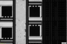
Automatic measurement solution (Wafer structure) |
> Learn more about PRECiV software
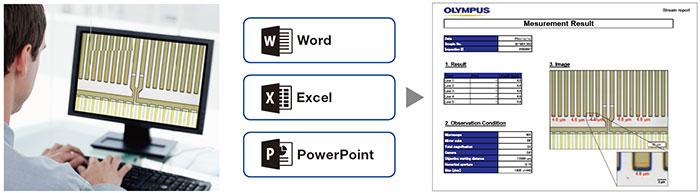
Efficient Report Creation
Creating a report can often take longer than capturing the image and taking the measurements. PRECiV software provides intuitive report creation to repeatedly produce smart and sophisticated reports based on pre-defined templates. Editing is simple and reports can be exported to Microsoft Word or PowerPoint software. In addition, PRECiV software’s reporting function enables digital zooming and magnification on acquired images. Report files are a reasonable size for easier data exchange by email.
> Learn more about PRECiV software
Advanced Designed to Support Cleanroom Conformity
The MX63 series is designed to work in a cleanroom and has features that help minimize the risk of contaminating or damaging samples. The system has an ergonomic design that helps keep users comfortable, even during prolonged use. The MX63 series complies with international specifications and standards, including SEMI S2/S8, CE, and UL.
Optional Wafer Loader Integration ― AL120 System*
An optional wafer loader can be attached to MX63 series to safely transfer both silicon and compound semiconductor wafers from a cassette to the microscope stage without using tweezers or wands. Renowned performance and reliability enable safe, efficient front and back macro inspections while the loader helps improve productivity in the laboratory.
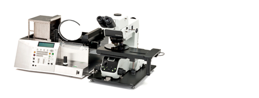
MX63 combined with the AL120 wafer loader (200 mm version)
* AL120 is not available in EMEA.
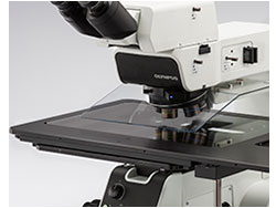
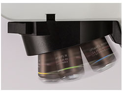
Fast, Clean Inspections
The MX63 series delivers contamination-free wafer inspections. All motorized components are housed in a shielded structure, and antistatic processing is applied to the microscope frame, tubes, breath shield, and other parts. The rotation speed of the motorized nosepieces is faster and safer than manual nosepieces, decreasing the time between inspections while keeping the operator's hands below the wafer, reducing potential contamination.
Antistatic breath shield |
Motorized nosepiece |
System Design Achieving Efficient Observations
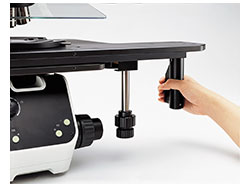
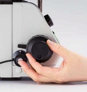
The XY stage is capable of both coarse and fine stage movements thanks to the combination of a built-in clutch and the XY knobs. The stage helps make observations efficient, even for large samples, such as 300 mm wafers.
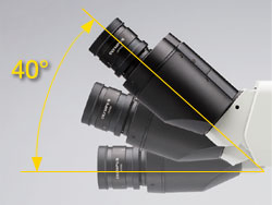
The tilting observation tube’s extensive range enables operators to sit at the microscope in a comfortable posture.
Stage handle with built-in clutch |
The tilting observation tube providing comfortable posture |
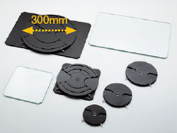
Accepts All Wafer Sizes
Wafer holders and glass plates | The system works with various types of 150–200 mm and 200–300 mm wafer holders and glass plates. Should the size of the wafters change on the production line, the microscope’s frame can be modified at minimal cost. With the MX63 series, different stages can be used to accommodate 75 mm, 100 mm, 125 mm, and 150 mm wafers on the inspection line. |
User-Friendly
Intuitive Microscope Controls: Comfortable and Easy to Use
The microscope’s settings are simple to operate, making it easier for users to make adjustments and reproduce system settings.
Find the Focus Quickly: Focus Aid
Inserting a focus aid in the optical path allows easy and accurate focusing on low-contrast samples, such as bare wafers.
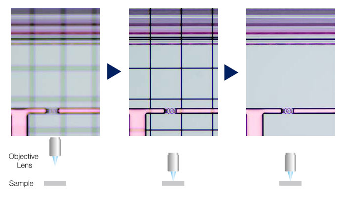
Left image: The grid indicates the image is out of focus. / Middle images: The grid assists focusing. / Right image: An in-focus image can be easily obtained.
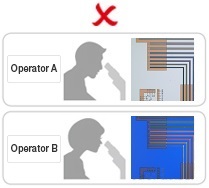
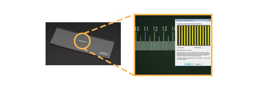
Easily Restore Microscope Settings: Coded Hardware
Coded functions integrate the MX63 series’ hardware settings with PRECiV image analysis software. The observation method, illumination intensity, and magnification are automatically recorded by the software and stored with the associated images. Since the settings can easily be reproduced, any operator can conduct the same quality inspections with minimal training.
|
|
|
|
| |
Different operators use different settings. | Retrieve the device settings with PRECiV software. | All operators can use the same settings. |


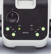
Ergonomic Controls for Quicker, More Comfortable Operation
The controls for changing the objective and adjusting the aperture stop are positioned low and in the front of the microscope so users don’t have to let go of the focusing knobs or move their head away from the eyepieces during use.
|
|
| ||
Centralized microscope operation | Hand switch | Snapshot button |
Faster Observations via the Light Intensity Manager and Automatic Aperture Control
In normal microscopes, users need to adjust the light intensity and aperture for every observation. The MX63 series enables users to set up the light intensity and aperture conditions for different magnifications and observation methods. These settings can be easily recalled, helping users save time and maintain optimal image quality.
Light Intensity Manger
| |
Conventional Light Intensity |
The image gets too bright or dark when changing magnification or observation method. |
Light Intensity Manager |
The light intensity is automatically adjusted to produce the optimal image when changing magnification or observation method. |
Automatic Aperture Control
| |
Maximum aperture: Higher resolution | Minimum aperture: Higher contrast and larger depth of field |
| |
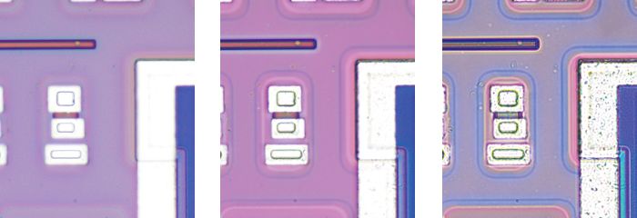

Image Quality
Exquisite Optics and Digital Imaging for Quality Inspections
Olympus history of developing high-quality optics and advanced digital imaging capability have resulted in a record of proven optical quality and microscopes that offer excellent measurement accuracy.
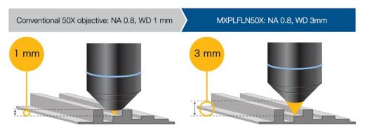
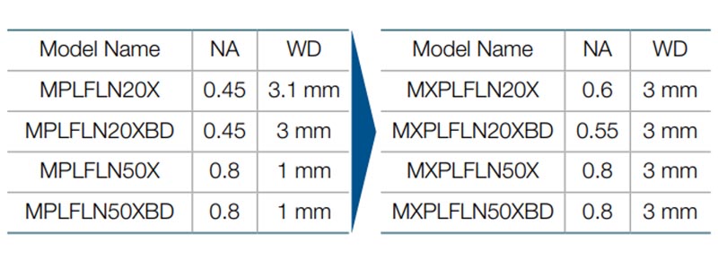
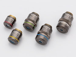
Combined high numerical aperture and long working distance
Objective lenses are crucial to a microscope’s performance. The new MXPLFLN objectives add depth to the MPLFLN series for epi-illumination imaging by maximizing numerical aperture and working distance at the same time. Higher resolutions at 20X and 50X magnifications typically mean shorter working distances, which forces the sample or objective to be retracted during objective exchange. In many cases, the MXPLFLN series’ 3 mm working distance eliminates this problem, enabling faster inspections with less chance of the objective hitting the sample.
|
|
> Learn More about MXPLFLN Objectives
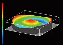
Superior Optical Performance: Wave Front Aberration Control
The optical performance of objective lenses directly impacts the quality of the observation images and analysis results. Olympus UIS2 high-magnification objectives are designed to minimize wavefront aberrations, delivering reliable optical performance.
Bad wave front |
Good wave front (UIS2 objective) |
> Click here for details about UIS2 objective lenses
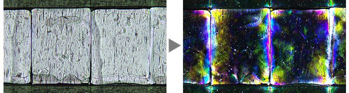
Consistent Color Temperature: High-Intensity White LED Illumination
The MX63 series utilizes a high-intensity white LED light source for reflected and transmitted illumination. The LED maintains a consistent color temperature regardless of intensity for reliable image quality and color reproduction. The LED system provides efficient, long-life illumination that is ideal for materials science applications
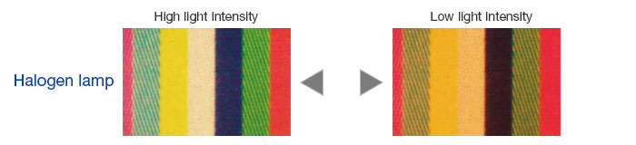
Color varies with light intensity.
Color is consistent with light intensity and clearer than halogen lamp.
* All images captured using auto exposure
Precise Measurements: Auto Calibration
Similar to digital microscopes, automatic calibration is available when using PRECiV software. Auto calibration helps eliminate human variability in the calibration process, leading to more reliable measurements. Auto calibration uses an algorithm that automatically calculates the correct calibration from an average of multiple measurement points. This minimizes variance introduced by different operators and maintains consistent accuracy, improving reliability for regular verification.
> Learn more about PRECiV software
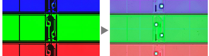
Entirely Clear Image : Image Shading Correction
PRECiV software features shading correction to accommodate for shading around the corners of an image. When used with intensity threshold settings, shading correction provides a more precise analysis.
Semiconductor wafer (Binarized image)
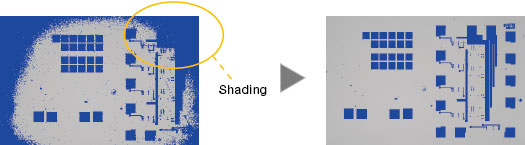
Right image: Shading correction produces even illumination across the field of view.
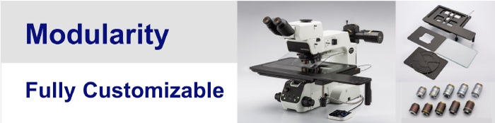
Modularity
Fully Customizable
The MX63 series is designed to enable the customer to choose a variety of optical components to suit individual inspections and application needs. The system can utilize all observation methods. Users can also select from a variety of PRECiV image analysis packages to suit individual image acquisition and analysis needs.
Two Systems Accommodate Diverse Sample Sizes
The MX63 system can accommodate wafers up to 200 mm while the MX63L system can handle wafers up to 300 mm with the same small footprint as the MX63 system. The modular design makes it easy to customize the microscope for your specific requirements
MX63 |
MX63L |
IR compatibility
Infrared observation can be conducted with the IR objective lenses, which enable the operators to nondestructively inspect the inside of IC chips packed and mounted on a PCB, utilizing the characteristics of silicon that transmit infrared light. 5X to 100X IR objectives are available with chromatic aberration correction from visible light wavelengths through the near infrared. Especially with an objective lens of 20X or more, the aberration caused by the silicon layer covering the observation object can be corrected by the correction collar to obtain a clear image.
IR objective lenses |
Without aberration correction |
With aberration correction |
Applications
The MX63 series is used in a range of reflected light microscopy applications. These applications are an example of some of the ways the system is used for industrial inspections.
IR image of an electrode section
Infrared (IR) is used to look for defects inside IC chips and other devices made with silicon on glass.
Film
(Left: Brightfield / Right: Polarized light)
Polarized light is used to reveal a material’s texture and the condition of crystals. It is suitable for inspections of wafer and LCD structures.
A hard disk
(Left: Brightfield / Right: DIC)
Differential interference contrast (DIC) is used to help view samples with minute height differences. It is ideal for inspections of samples having very minute height differences such as magnetic heads, hard-disk media, and polished wafers.
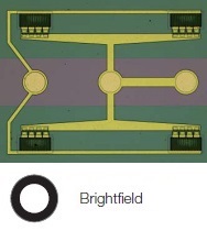
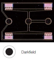
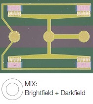
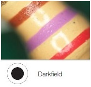
IC pattern on a semiconductor wafer
(Left: Darkfield / Right: MIX (Brightfield + Darkfield))
Darkfield is used for detecting minute scratches or flaws on a sample or inspecting samples with mirrored surfaces, such as wafers. MIX illumination enables users to view both patterns and colors.
Photoresist residue on a semiconductor wafer
(Left: Fluorescence / Right: MIX (Fluorescence + Darkfield))
Fluorescence is used for samples that emit light when illuminated with a specially designed filter cube. This is used to detect contamination and photoresist residue. MIX illumination enables the observation of both the photoresist residue and IC pattern.
An LCD color filter
(Left: Transmitted Light / Right: MIX (Transmitted Light + Brightfield))
This observation technique is suitable for transparent samples such as LCDs, plastics, and glass materials. MIX illumination enables the observation of both the filter color and circuit pattern.
Specifications
| MX63 | MX63L | ||
| Optical system | UIS2 optical system (infinity-corrected system) | ||
| Microscope frame | Reflected light illumination |
White LED(with Light Intensity Manager) 12 V 100 W halogen lamp, 100W mercury lamp, light guide source
Brightfield/darkfield/mirror cube manual changeover. (Mirror cube is optional.) 3 position coded mirror units changed by manual operation Built-in motorized aperture diaphragm (Pre-setting for each objective, automatically full open for darkfield) Observation mode: brightfield, darkfield, differential interface contrast (DIC)*1, simple polarizing*1, fluorescence*1, IR and MIX observation(4 directional darkfield)*2 *1 Optional mirror cube, *2 MIX observation configuration is required | |
| Transmitted light illumination |
Transmitted light illumination unit: MX-TILLA or MX-TILLB is required.
- MX-TILLA: a condenser (NA 0.5) and an aperture stop - MX-TILLB: a condenser (NA 0.6), an aperture stop and a field stop Light source: LG-LSLED (LED light source) Light guide: LG-SF Observation mode: brightfield, simple polarizing | ||
| Focus |
Stroke: 32 mm
Fine stroke per rotation: 100 μm Minimum graduation: 1μm Upper limit stopper and torque adjustment for coarse handle | ||
| Maximum load weight (including stage and holder) | 8 kg | 15 kg | |
| Observation tube | Wide-field (FN 22 mm) |
Erect and trinocular: U-ETR4
Erect, tilting and trinocular: U-TTR-2 Inverted and trinocular: U-TR30-2, U-TR30IR (for IR observation) Inverted and binocular: U-BI30-2 Inverted, tilting and binocular: U-TBI30 | |
| Super-wide-field (FN 26.5 mm) |
Erect, tilting and trinocular: MX-SWETTR (optical path switchover 100% (eyepiece) : 0 (camera) or 0 : 100%)
Erect, tilting and trinocular: U-SWETTR (optical path switchover 100% (eyepiece) : 0 (camera) or 20% : 80%) Inverted and trinocular: U-SWTR-3 | ||
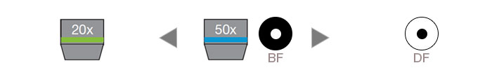
| Motorized nosepiece | Brightfield Brightfield and darkfield | ||
| Stage (X × Y) | Coaxial right handle with built-in clutch drive: MX-SIC8R Coaxial right handle with built-in clutch drive: MX-SIC6R2 |
Coaxial right handle with built-in clutch drive: MX-SIC1412R2
Stroke: 356 x 305 mm Transmitted light illumination area: 356 x 284 mm | |
| Weight | Approx. 35.6kg(Microscope frame 26kg) | Approx. 44kg(Microscope frame 28.5kg) | |