Near-infrared (NIR) imaging using a microscope can image through silicon up to 650 μm thick, making it a powerful way to inspect electronics and semiconductors. A typical microelectronics failure-analysis protocol requires the ability to nondestructively inspect circuit patterns through silicon while maintaining the mechanical integrity of the finished product.
Typical electronics inspections using NIR imaging include:
- Inspection for short circuits within the product (e.g., burnout marks, stress indicators)
- Bonding alignment (analysis of alignment marks between thinly bonded circuits and alignment of bonded wafers)
- Inspection after electrical testing (any type of failure)
- Assessment of chip damage (e.g., defects in materials, contamination)
- Inspection of microelectromechanical systems (MEMS), such as the structure of the device within bonded wafer, detection of voids and defects, and imaging of live mechanical movement
Read on to explore examples of how NIR imaging is used for electronics and semiconductor inspections. Plus, learn about the industrial microscopes, digital cameras, and objectives that support NIR imaging in these applications.
Examples of How NIR Imaging Is Used for Electronics and Semiconductor Inspections
NIR imaging enables you to perform microscope inspections of electronic parts that cannot be seen visually. Here are some of the powerful ways NIR imaging is used in industrial inspections:
1. Inspect chip damage in wafer-level chip-scale packaging (CSP).
A wafer-level chip-scale package is an integrated circuit package at the wafer level. NIR imaging using a microscope can be used to nondestructively inspect chip damage that occurs during heat and moisture tests. An IR microscope can image through silicon so you can observe leakage from melting, corrosion of copper wiring, peeling of resin parts, and other issues.
2. Perform nondestructive flip-chip analysis.
As the name suggests, a flip chip is a chip packaging method where the active area of the chip is flipped over and mounted directly onto a substrate, board, or carrier. Once the flip chip is bonded to the part, the chip pattern can’t be inspected using visible light. In contrast, an IR microscope enables you to look through the silicon to check for defects to the interior without destroying the mounted chip. This is also an effective way to identify the areas that should undergo focused ion beam (FIB) processing.
3. Determine the amount of wafer grinding.
Wafer grinding is a semiconductor device fabrication step that reduces the wafer thickness. The thinning of devices by grinding increases the need to measure both sides of the wafers. Yet, it is extremely difficult to measure the grinding amount on both sides of the laminated wafers. An IR microscope system can image through the material to focus on the front and back of the wafer, enabling you to obtain the general distance. Then you can determine the extent of the grinding by measuring the amount of Z-movement of the objective.
4. Determine the chip gap in 3D mounting configurations.
IR microscopes can also assist with silicon gap management. The chip gap in a three-dimensional (3D) mounting configuration can be nondestructively determined by measuring the amount of movement of the objective when IR light passes through the silicon and focuses on the chip and interposer. This method can also be used in the measurement and hollow construction of MEMS devices.
5. Image a range of difficult samples.
Shortwave-infrared (SWIR) imaging at longer wavelengths—for example, the 1300–1500 nm range—enables imaging on more difficult samples such as MEMS devices, heavily doped silicon samples, samples with rough surfaces, wafer bonding, and 3D chip stacks. This method is possible using more sensitive imaging systems, such as indium gallium arsenide (InGaAs) cameras. The signal benefits from dedicated IR objectives, high-power illumination, and InGaAs cameras during reflected- or transmitted-light microscopy enables imaging on these more difficult samples.
Tools for NIR Imaging: Industrial Microscopes, Near-Infrared Cameras, and More
A range of tools are available to enable near-infrared imaging in quality control and research and development (R) laboratories. This includes:
1. Transmitted-light IR microscopes
Reflected-light microscopy is ideal for illuminating a sample from above. In comparison, transmitted-light IR microscopy brings light to a sample through silicon from beneath the sample, providing higher contrast. Transmitted-light microscopy is especially useful for inspecting alignment patterns or fiducial marks through silicon.
Our MX63 microscope offers transmitted-light IR observation for nondestructive inspections of defects inside IC chips and other electronic devices constructed with silicon or glass that easily transmit IR wavelengths of light.
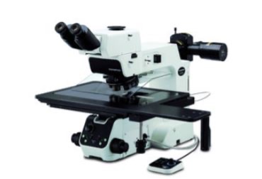
MX63 inspection microscope for semiconductors and flat panel displays
2. Near-infrared cameras
Digital microscope cameras can provide high-contrast images throughout the NIR spectrum up to 1100 nm while still maintaining a large field of view. Our DP23M monochrome microscope camera paired with a 1100 nm bandpass (BP) filter offers a broad spectral response from visible light up to 1100 nm, making the camera ideal for NIR imaging. With 6.4-megapixel resolution, the camera provides dependable, high-quality gray scale and infrared microscopy images.
Here are some examples below:
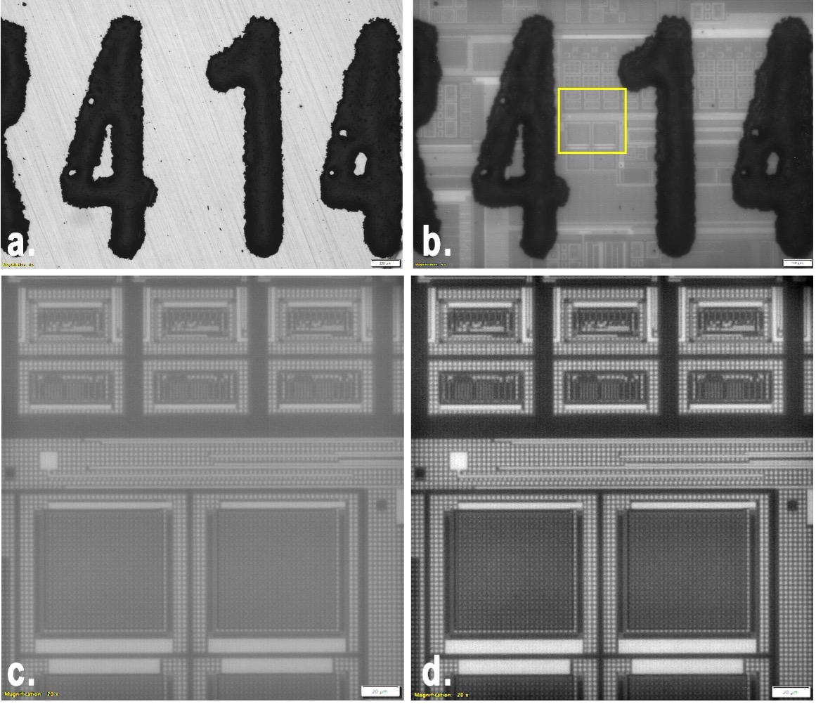
Images of a semiconductor chip captured using the DP23M digital microscope camera. A) Brightfield image 5X. B) IR image 5X (BP1100 nm filter). C) Cropped detail 20X IR. D) Cropped detail 20X IR with a differential contrast enhancement (DCE) filter.
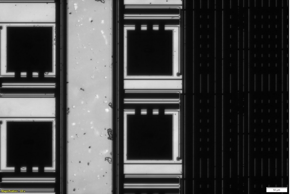
Transmission IR image (10X) of a semiconductor chip. Captured using the DP23M digital microscope camera.
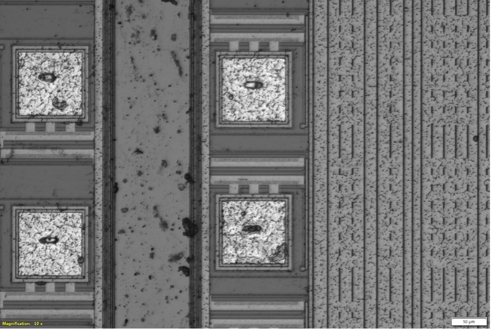
Brightfield image (10X) of the same semiconductor chip shown above. Captured using the DP23M digital microscope camera.
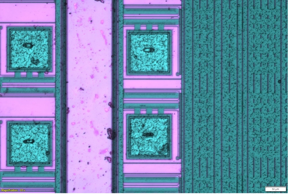
Providing enhanced contrast on the sample, an overlay image in false colors represents the brighter areas and darker areas on the semiconductor chip. Brightfield (cyan blue) and transmission IR (magenta). Captured using the DP23M digital microscope camera.
3. Near-infrared objective lenses
The latest NIR objective lenses can provide increased transmittance at the NIR spectrum. Correction collars on our LCPLN-IR 20X, 50X, and 100X objectives can be set for a specific silicon thickness for improved transmittance, contrast, and aberration correction.
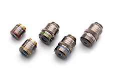
LCPLN-IR objectives for inspecting internal structures in silicon wafers
4. Image analysis software
Most failure-analysis and R laboratories demand a digital approach to measuring defects, creating reports, and archiving images. Because of the nature of this application (imaging through the material with low light), native contrast is minimal and must be optimized through image analysis software. Uneven illumination from causes such as vignetting darkens the image corners relative to the center. This must be digitally removed from the live view and captured image.
Dedicated software can solve these challenges, providing:
- Live shading correction to maximize image uniformity across the field of view
- Accurate measurements anywhere within the field of view
- Automatically generated reports
- Archiving of images and relevant data
Our IR microscopes and digital cameras integrate with PRECiV™ image and measurement software to create a seamless inspection workflow from imaging to reporting. To learn more about our solutions for NIR imaging, reach out to our experts today.
Related Content
DP23M Industrial Microscope Camera
Controlling Quality Control in Electronics Manufacturing Using PRECiV Software