Microelectronic components in electronics have become part of our daily life—whether in smartphones, smart homes, or smart cars. Built with intelligent optical sensors and emitters, as well as corresponding logic and memory modules, these advanced components require highly developed production facilities with special care in handling and quality control. As a result, semiconductor wafer production is largely an automated process. However, some parts of production are supplemented with manual test processes, such as microscopy, in a controlled cleanroom environment.
Meeting Quality Requirements in LED Production Using Microscopy
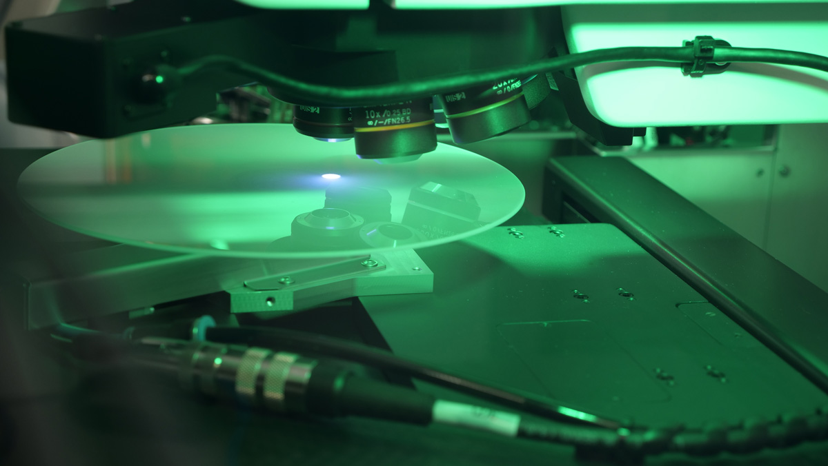
Figure 1. Sapphire wafer under an MX series microscope. Image courtesy of PVA SPA.
Microscopy helps manufacturers meet quality requirements in LED production. The demand for higher output and reliable end products drives the continuous improvement process in LED production. Advances in miniaturization and increases in power density require these improvements.
ams OSRAM is a leading manufacturer of optical solutions dedicated to meeting strict production requirements. Its opto-semiconductor business in Regensburg, Germany, has high-quality standards for air purity and protection against particle contamination at visual post-control stations. Microscope systems for the post-control of sapphire, gallium arsenide (GaAs), or silicon wafers in LED production are usually open workplaces in a cleanroom certified to the DIN EN ISO 14644-1 standard.
To reduce the generation of particles by the plant operator, wafers must be shielded during microscopic inspection. A defined air purity is also set within the inspection system. The wafers are transported between the different process steps in closed cassettes with 25 parts each to meet the increased demands. Consequently, a machine must be able to unlock this cassette and lock it again at the end of the process. For wafers with a diameter of 200 mm (7.9 in.), SMIF (Standard Mechanical Interface) cassettes are used. Most of the time, the visual inspection of the wafer’s surface properties is performed using lithographic and chemical processes. The plant operators must confirm the size of the components are accurate and determine the absence of defects.
Microscope System Integration for Automated Production
To meet these requirements, ams OSRAM needed to find a supplier for partially automated microscope systems with an integration process suitable for automated production. The manufacturer turned to PVA TePla, a system engineering company represented by the subsidiary PVA SPA Software Entwicklungs GmbH based in Coburg, Germany.
PVA SPA provided high flexibility when implementing their special process requirements. This included standardized plant coupling using the SECS-GEM protocol and full traceability of manual optical controls through digital reporting to a higher-level production control system. PVA SPA provided individual solutions for these needs. The new semi-automated microscopes provided by the supplier could also meet a corresponding profitability test carried out by the manufacturer.
Together, the guided wafer inspection and simple operator control form a well-integrated manual solution in the automated production environment. The production and data control systems are automatically filled after the partial manual control. The line flow and booking ways are only slightly affected.
Intelligent Microscope Systems for Wafer Inspection
The newly designed microscope system includes a UL200 wafer loader that can automatically open and relock SMIF wafer cassettes. After unlocking, the wafers are loaded from the cassette into an enclosed interior space within the system. Here, a flow box located on the housing provides a downward laminar flow of pure air, as adequate air purity in the system interior is essential. The housing of the wafer loader and microscope also protects the components from mechanical damage.
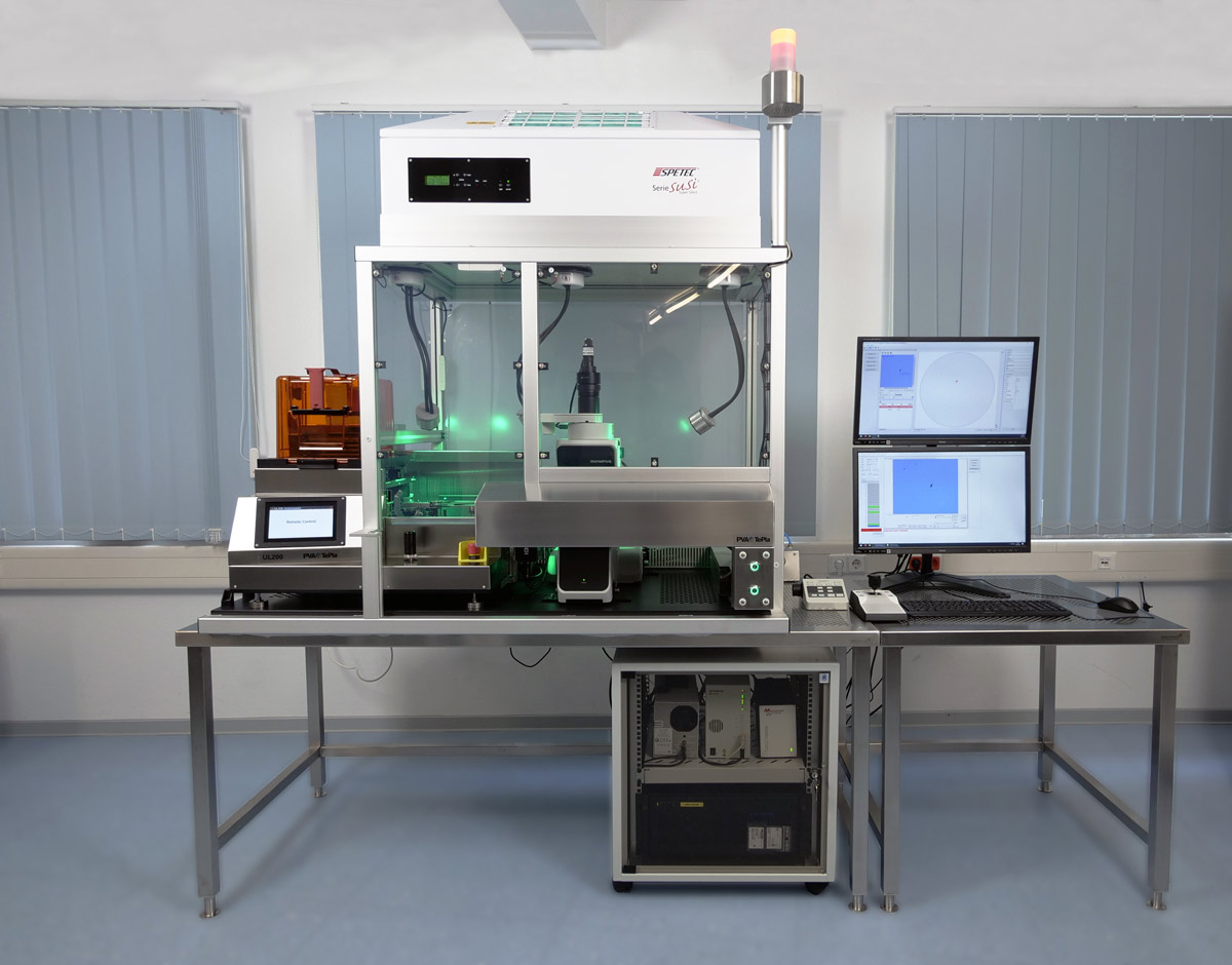
Figure 2: Microscope system integrates a UL200 wafer loader for SMIF wafer cassettes and a flow box for air purity. Image courtesy of PVA SPA.
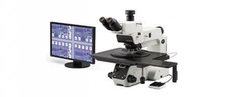
The system integrates the Olympus MX™ series semiconductor inspection microscope. This microscope features a modular, integrable laser autofocus and motorized XY table that can be completely controlled from the outside. This enables operators to process defined inspection tasks from the screen.
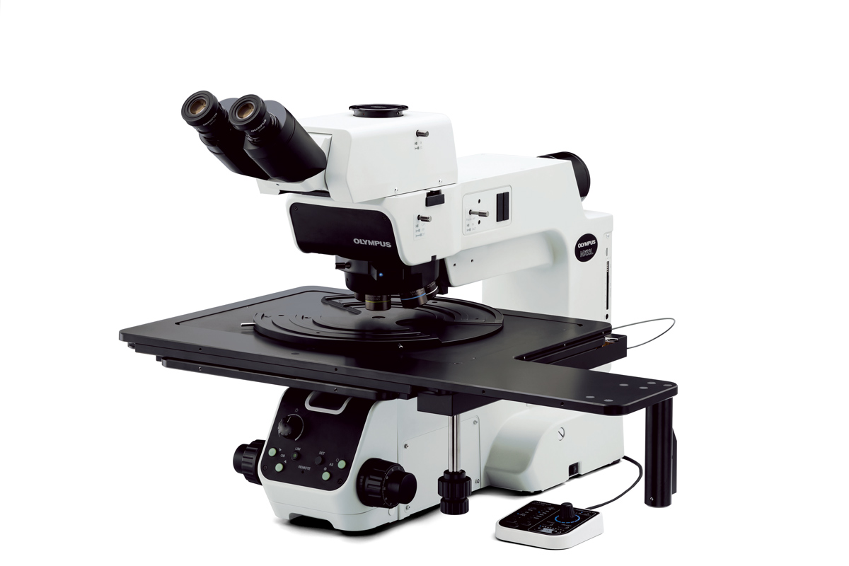
Figure 3. MX series semiconductor microscope can be used to inspect wafers up to 300 mm (11.8 in.)
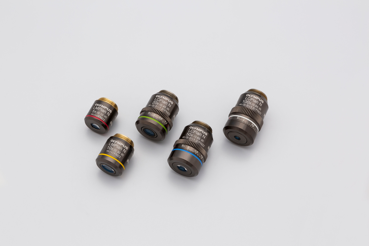
Figure 4. High-quality objective lenses used with the MX series microscope are ideal for UV fluorescence and infrared inspection.
For the traceability of defects found on a wafer, operators can measure the abnormalities in the image and add the digital information to KLARF files, an industry standard format for extended wafer map functionalities. For process improvement, the MX series microscope can also target defects on the wafer. In the past, these defects were found using automatic optical inspection (AOI) systems.
Enabling Analytical Work in an Automated Process Environment
Even with the latest AOI system, the manual optical controls from the microscopes are indispensable for ams OSRAM. Manual efforts are often needed for development and product improvement. Dr. Robert Friedemann, Key Expert, Testing and Analytics at ams OSRAM, explains the advantages of these manual controls on product development and quality.
"With the SMIF microscopes, we have succeeded in providing our engineering and development colleagues with a control system that enables analytical work in an automated process environment,” says Robert. “A macroscopic and microscopic impression of the wafer material is indispensable for basic developments and product improvements. The markings and images are now linked directly in KLARF and can be viewed immediately in the yield management system at the corresponding process stage."
PVA SPA remained flexible throughout the entire process to make sure all needs were met. For instance, various bandpass filters need to be steered and controlled by the software. Further, the LEDs of the microscope illumination must be individually controllable for spectral microscopy.
“Sometimes a system needs to be respecified. As a system integrator, it is essential to always remain flexible and open to individual customer needs, “ says Kevin Fredriksen, Sales Director at PVA SPA.
Robert and Kevin agree that the microscope system meets all the identified needs and provides a reliable, cost-effective solution for product development and quality.