Wafer inspection is a key process in the semiconductor industry that involves finding defects on a wafer. Put simply, a wafer is a thin slice of semiconductor material, such as silicon, used to make integrated circuits (also called ICs or chips) where electric circuits are mounted.
Semiconductor chips are essential components in electronic devices such as cars, laptops, appliances, and smartphones, so wafers are produced quickly and in large numbers. To keep up with demand, wafer inspection must be fast, accurate, and repeatable.
So, how can manufacturers improve their wafer inspection quality control?
One easy way to optimize your wafer inspection process is to choose the right combination of equipment. Pairing a semiconductor wafer inspection microscope with intuitive metrology image analysis software can simplify your workflow and save time. This post covers how to optimize your microscope setup and workflow for wafer inspection and defect analysis.
Tips to Select Microscope Equipment and Software for Wafer Inspection
Wafer manufacturing is a complex process. It includes circuit creation, wafer oxidization, photoresist coating, pattern printing, etching, impurity diffusion, and planarization. Defects can be introduced into the final products at any of these stages. Common defects include irregular coatings, impurities, and broken circuits.
Wafer defects can prevent the electric circuit from functioning properly, so wafer inspection is a critical step to ensure product quality in the manufacturing process. With defects at the micrometer scale, optical microscopes are often used for nondestructive wafer inspection. You should be able to clearly view the sample surface with various observation methods and objective lenses, as well as easily document results for further analysis or future reference.
Microscopes equipped with motorized stages and wafer navigation software help this work go as quickly as possible. Look for optical microscopes that offer fast image measurement technology by combining advanced hardware and analysis software.
The hardware you choose depends on your applications. Semiconductor wafer inspection microscopes are available that support 4-inch, 8-inch, and 12-inch wafers. For example, our MX63L microscope is equipped with a large stage to accommodate wafers as large as 12 inches.
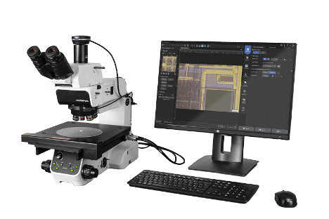
Figure 1. MX63L microscope for wafer inspection
Wafer inspection microscopes can be paired with various high-resolution digital cameras and infrared (IR) cameras. Together with modern metrology software, wafer inspection microscopes can:
- Capture high-resolution, sub-micrometer wafer images at various locations
- Perform measurements
- Provide OK/NOK judgements
- Save all data
Some systems even offer guaranteed measurement accuracy and repeatability so that you can be confident in the results.
Perform an Efficient Wafer Inspection Using Predefined Workflows
Another important capability for an optimized wafer inspection setup is automation. As metrology inspections are typically performed at multiple known positions on a wafer, automating this process greatly improves inspection efficiency. Yet, one of the most time-consuming parts of setting up the automation is programming the software to carry out the repeated inspections.
When choosing metrology software, look for one that offers predefined workflows. This feature enables you to quickly and easily set up an automated inspection. Likewise, make sure the hardware you choose can locate the inspection positions quickly and accurately. For example, this optimized setup can be achieved by combining our MX63L microscope with PRECiV™ image and measurement software.
Types of Automated Wafer Inspections
Automated wafer inspections can be set up in different ways depending on the information available to you. Here are two options:
1. Wafer inspection with a known wafer layout
Since wafers are predesigned, manufacturers normally have a corresponding map layout file describing the 2D structures on different chips. In CAD files, it is even possible to save Z-height information of each point for a 3D structure layout. This layout file can be used to build the wafer navigation map if you are using metrology software that can read these files. To do this, open the wafer design file in CAD software and define the points of interest on the chip. Save this information and then transfer it to your metrology software.
Many modern metrology software programs can read CAD files (e.g., DXF files) and transfer the points the user programmed, as shown in Figure 2a below. In this example, the green lines represent the circuit’s design on the wafer. The wafer markers (exaggerated: ×, +, and o) are used to align the wafer (on some wafers only one pair of markers is available or the markers are in reverse order). Note that an optional third reference point on the wafer enables you to perform tilt correction.
(a)
(b)
Figure 2. (a) Example CAD drawing of a wafer and (b) images captured using an MX™ microscope and PRECiV software at the locations defined in image (a).
Users must confirm the two or three points’ locations and their focus in the software every time they load a new wafer. After, the software will drive the motorized stage to move to all predefined measurement points (red dots in Figure 2a) to capture in-focus images or perform live analysis. Figure 2b shows the individual images that the hardware and software captured. They look almost the same since the points of interest are in the same locations on different chips.
Users can easily modify the positions in the original definition file and transfer the updated file to the metrology software to modify the imaging process. Choose a metrology software vendor that will work closely with you to help adjust and review all CAD files so that the software meets your specific inspection workflow.
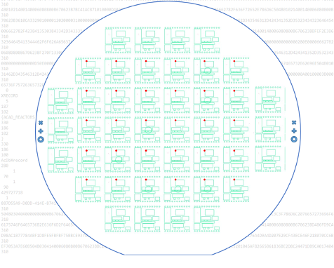
2. Wafer inspection with row- and column-based positioning
For users without a CAD drawing of the wafer layout, some image analysis programs offer a multiposition and repetitive measurement workflow. One example is the Navigate on Wafer customized solution in PRECiV software. The solution defines the wafer layout and navigates to various points on the wafer for imaging. Figure 3 shows an example specifying multiple sample regions.
First, the wafer layout (chip offset in x and y) as well as the alignment can be defined by three given chip positions. Users must pick up the repetitive structures (blue dots in Figure 3) in different chips, such as (3,3), (3,8), and (7,8).
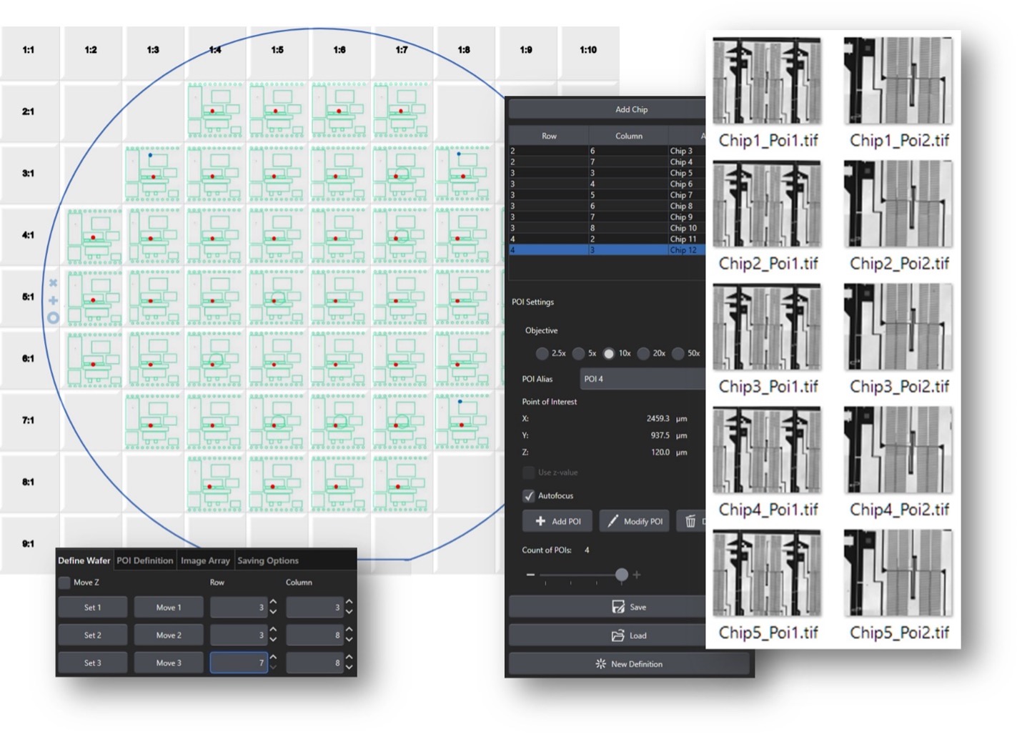
Figure 3. Schema of a wafer sample. Layout definition is row- and column-based using three chips (blue dots). The defined points of interest (POIs) are the red dots (left). Sample images (right) are shown on POIs.
The exact coordinates of each chip will be defined based on this coordinate system. Then, users must define a chip list and points of interest (POIs) per chip. This includes determining specific locations on the chip and objective lenses for acquisition per POI (10X, 20X, 50X, etc.) and choosing whether to apply autofocus at each location. The settings will be accessed for all subsequent automatic movements to different chip positions.
To see how the Navigate on Wafer solution works in action, watch the video below:
Defect Analysis on Blank Wafers
Checking blank wafers for impurities is another important inspection. This testing can be challenging because the microscope must acquire—and the software must process—a large number of images. Fast multiposition image acquisition software capabilities benefit this inspection.
To detect particles, some metrology software enable users to set up a phase threshold to identify impurities. Other particle restrictions—such as shape and size limitations—can be set up as well. Phase analysis, particle counts, and size distributions can also be performed simultaneously with impurity detection. Figure 4 shows an example of metrology software detecting impurities on a contaminated sample and then displaying them in an Excel spreadsheet.

Figure 4. A snapshot image of a blank wafer sample showing impurities in PRECiV software. Imaged with an MX microscope and monochrome camera from Evident.
Another reason wafer inspection can be slow is the sheer number of images that need to be captured. Capturing the images separately, processing them one after another, and saving them is slow and inefficient. Each step takes time, image storage takes up a lot of space, and human effort is involved at each step. In addition, under certain circumstances (e.g., repetitive measurements), the images all tend to look the same. Users are only interested in the images that contain relevant data, so there is rarely a need to save all of them.
Modern metrology software can combine multi-image-alignment acquisition with live image processing (phase analysis) for impurity detection on the resulting stitched image. A typical workflow includes the following steps:
- Load a wafer sample
- Perform the stitching acquisition process
- Set up a threshold
- Click the Particle Detection button
Additionally, users can define some pass criteria, so the software can make a judgement about which particles to consider.
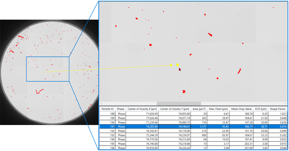
Figure 5. Particle detection on a stitched image of an (exaggeratedly) contaminated wafer sample (left). A magnified section of the image with a tabular display of the detected particles is shown on the right.
The table in Figure 5 above shows the results of live particle detection on the stitched image. If your microscope is equipped with a motorized stage, clicking on a particle in the image or clicking on the results in the table will drive the stage to the particle location on the sample so that you can confirm what the software detected. To facilitate the search for large particles, each table column can be sorted.
As an alternative to conventional threshold-based analysis, deep learning can speed up particle detection on wafers while offering higher reproducibility and a more robust analysis. You can learn more about how deep learning makes image analysis easier and more accurate in our post, The Potential of AI-Based Image Analysis in Metallography and Materialography.
Making Wafer Inspection as Efficient as Possible
Semiconductor wafer manufacturers continue to explore ways to speed up all their processes, including quality control. This post demonstrates that choosing the right combination of microscopy hardware and metrology software is important for making wafer inspection as efficient as possible. Modern features, such as easy-to-use multiposition imaging, real-time analysis, and deep learning, greatly simplify and speed up the inspection process while providing repeatability and accuracy. Tailoring the analysis software to specific wafer navigation and measurement needs can further streamline inspections.
If you need assistance optimizing your wafer inspection microscope and workflow, simply reach out to one of our experts. We’re here to help!
Related Content
Controlling Quality Control in Electronics Manufacturing Using PRECiV Software
Capabilities of Near-Infrared Imaging for Electronics and Semiconductor Inspection
Mix Observation Methods to See More in Your Wafer Defect Inspection