Executive Summary
Moving towards sustainable manufacture of photovoltaics, Dr Manuela Schiek’s research group in Oldenburg has discovered how the latest technology in confocal laser scanning microscopy is enhancing both accuracy and efficiency of their research into organic semiconductors and transparent electrodes.
Harvesting energy directly from the sun in order to generate electricity, solar cells appear to represent the epitome of green energy. But have you ever stopped to consider the manufacturing process? Take the case of crystalline silicon for example, a main component of conventional solar cells. Firstly, transforming silica ore into its valuable crystallised form requires temperatures of above 2,000°C. Not only is this an incredibly energy-hungry process in itself, but obtaining ultra-pure
silicon also involves several hazardous chemicals and a potent greenhouse gas. Other main offenders in the modern manufacture of many inorganic thin-film solar cells include components comprising the toxic elements selenium and cadmium. Indium is also a vital ingredient, forming indium tin oxide (ITO), but reserves of this finite resource are estimated to become unviable by 2017, which poses another set of potential challenges. Take the case of tantalum, for example: vital for the creation of
electrical transistors, the limited availability of this contentious material sits at the heart of political conflict in the Democratic Republic of Congo.
With the increasing strain on the global power grid and the drive towards sustainable energy production, we must therefore ensure that methods of manufacturing green-energy devices are equally sustainable – and this is the goal of Dr Manuela Schiek’s research group at the University of Oldenburg. Their research focuses on alternative materials for solar cell manufacture that are both non-hazardous and readily available. This includes the use of organic semiconductors within the
energy-capturing active layer, and a transparent electrode system formed from a silver nanowire mesh embedded in an organic polymer matrix (see text box “organic solar cell architecture”).
With its complex multi-layered structure, surface analysis techniques provide vital insights into the workings of a solar cell. While tactile profilometry and Atomic Force Microscopy (AFM) have been the mainstays of surface metrology for a number of years, 3D confocal laser scanning microscopy (CLSM) is becoming an ever more popular tool.
Combining the ability to generate detailed, true-colour optical images with the non-contact capabilities of laser scanning technology, the confocal laser scanning microscope really comes into its own as an optical profilometer. Faster and more efficient than stylus-based techniques, 3D CLSM is able to measure soft or adhesive surfaces and offers a resolution of 0.2 µm. Offering such benefits, the recent introduction of an Olympus LEXT OLS4100 3D confocal laser scanning microscope into Dr
Schiek’s laboratory has greatly enhanced their research into alternative means of photovoltaic manufacture.
Organic solar cell architecture
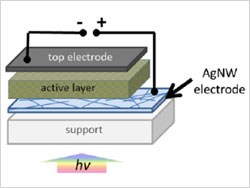 | The most popular organic solar cell architecture is based on a photon-harvesting active layer, sandwiched between two electrodes – one of which must be transparent in order to allow light to penetrate. Photons hitting the organic semiconductor generate the charge-carrying excitons, which by the use of two materials – an electron donor and an electron acceptor - are then separated into their separate electron and holes. Driven by an
electrical field,the electrons and holes travel toward their respective electrodes, creating the charge separation necessary to form an electrical circuit.
Dr Schiek’s research looks at using a transparent silver nanowire (AgNW) mesh electrode to replace the brittle and rare ITO, in addition to forming the active layer from organic materials as an alternative to environmentally damaging chemicals – creating flexible, sustainable and affordable thin-film solar cells for consumer applications. |
Organic materials in the active layer
The active layer is where energy is captured from photons, and within organic solar cells this is often formed from a discontinuous blend of two materials – a polymer and a fullerene. With the polymer acting as an electron donor and the fullerene as an electron acceptor, this bulk heterojunction structure leads to enhanced charge separation of electrons and holes, and hence improved solar cell function. But polymers are often roughly defined mixtures of material with differing chain
lengths, and with properties that are highly batch-specific. Molecular semiconductors, on the other hand, are defined building blocks with properties that can be adjusted by small changes to their structure, which can therefore be optimised for improved solar cell function. An interesting class of such molecules are the squaraine dyes (Figure 1), whose structure gives a broad absorption in the red region of the light spectrum. Dr Schiek’s research is investigating a bulk heterojunction
active layer formed from squaraines mixed with a fullerene acceptor (for more information, see reference 1). The thickness of the active layer is crucial for this application: too thin and the mobility of charge carriers is restricted, but too thick and both light absorbance and flexibility are significantly reduced.
Accurate measurement of layer thickness is therefore equally important. Within Dr Schiek’s laboratory, once a scratch is made through the active layer surface with a fine needle, the step edges of this ‘valley’ are subsequently measured using profilometry. Tactile profilometry was previously relied upon, but the softness of the organic material hampered accurate measurement. In fact, a height discrepancy of around 20 nm was frequently observed between the two step edges, which
is significant considering the average thickness of the active layer is 100 nm. As the needle steps up from the valley, it scratches into the surface and results in the false lower height reading.
With 3D confocal laser scanning microscopy, it is the laser that scans the surface, and such a non-contact approach achieves far greater accuracy of surface profilometry (Figure 2). Moreover, providing a visual image of the sample is more intuitive, and with the LEXT OLS4100 this information is easily compiled into a report, presenting the image in support of numerical data (Figure 2B).
Squaraines under polarised light.
These molecular dyes present a sustainable alternative for the active layer, here visualised between crossed polars with the Olympus LEXT OLS4100.
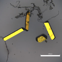 Figure1.A: single crystals exhibit a golden metallic lustre; | 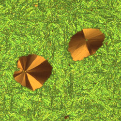 Figure1.B: a spincoated layer of neat squaraine, with spherulite aggregates forming through crystallisation upon thermal annealing. |
Accurate metrology of soft material.
Formed from soft organic material, the active layer is typically 100 nm thick and easily damaged by contact.
 Figure2.A: Non-contact profilometry is here achieved with the Olympus LEXT OLS4100 | 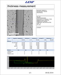 Figure2.B: Data compiled into a report. |
Transparent electrodes
Combining optical transparency with conduction, transparent electrodes form the anode of the solar cell while also allowing light to pass through to the active layer. The rapidly diminishing resource of ITO is currently the industrial standard for transparent electrodes. Moreover, ITO is a brittle material, restricting its use in mechanically flexible devices, and the hunt is on for a lightweight, cheap, flexible alternative that is also compatible with large-scale processing. Graphene presents
a potential alternative, for example (Figure 3), but the flakes are quite small, which limits its use for larger areas.
One promising alternative is a mesh of silver nanowires (AgNWs) embedded in a polymer matrix, and a second project within Dr Schiek’s laboratory focuses on the production of the AgNWs, the subsequent processing to form the electrodes and ultimately the integration into organic solar cells.
For optimum conductivity, a uniform connection must exist between the active later and electrode, demanding a homogenous AgNW mesh. Since the diameter of AgNWs at 100 nm is equivalent to the thickness of the active layer, it is also important to avoid these regions of aggregation and to prevent puncturing the active layer. However, in practice this is challenging to achieve across the whole solar cell using current spin-coating production techniques, and surface roughness evaluation plays a
central role in optimising the synthesis protocol.
AFM has been the main technique employed for the surface roughness evaluation of the AgNW mesh, but the introduction of the LEXT OLS4100 has vastly improved the efficiency of this. Firstly, Dr Schiek found that expanding the field of view using the image stitching function allowed her to view a more representative sample of the electrode surface. The AgNW mesh may appear regular on a smaller scale, but by creating high-resolution images of one mm2 (ten times greater than possible with AFM),
regions of aggregation are easily identified that would otherwise have been missed (Figure 4A,B). As can be seen in Figure 4C, the software also allows the height profile to be visualised in 3D, useful for both analysis and documentation. Moreover, the ability to increase the low-pass filter from a height of 80 µm to 800 µm allows more insightful analysis of the elevated regions of the silver nanowires.
It is also the case that AFM is time consuming. Not only does the scan itself take up to an hour, after setting up the instrument and adjusting for tip-related artefacts, it can often take a whole day to acquire a single useful image. With 3D CLSM, image acquisition is rapid and also highly intuitive owing to the dedicated software, even for students lacking microscopy experience. In terms of performance, the researchers found that AFM and CLSM with the LEXT OLS4100 produced comparable results,
and have benefited from the improved efficiency of surface roughness evaluation of transparent electrodes.
Another interesting aspect of this project is the far-reaching potential of transparent electrodes throughout opto-electronic applications, including LEDs and touch screens, where developing alternatives to ITO is also a focus of intense investigation. In the future, opto-electronic interfaces might even enable sight restoration, with retinal implants using light to generate electrical output and stimulating neuronal activity.
A flake of multilayer graphene coated with a light emitting organic semiconductor.
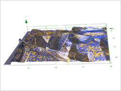 Figure3 | This structure is currently under investigation for organic light emitting diodes, while graphene also has potential for use as a transparent electrode – although flakes are too small for larger photovoltaic surfaces. Visualised with crossed. |
Surface roughness evaluation of silver nanowire mesh electrodes using the Olympus LEXT OLS4100.
Image stitching function expands the field of view, Low-pass cut-off filter set to 800 µm.
 Figure4.A: facilitating analysis of nanowire distribution on a larger scale in brightfield. | 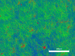 Figure4.B: Height colour plot. |
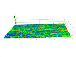 Figure4.C: Organic solar cell architecture | |
Summary
Feeding the global power grid in a sustainable fashion remains one of the biggest challenges faced by the modern world, and it’s an exciting time for research into innovative solutions. The use of widely available materials holds future promise in providing a green alternative to conventional solar cell manufacture, with such investigations driven by the latest technological developments.
From enabling accurate step measurements of the active layer with non-contact profilometry, to improving the efficiency of analysis with speed and advanced software functions, the Olympus LEXT OLS4100 3D confocal laser scanning microscope has provided Dr Manuela Schiek’s research group with many advantages over stylus-based methods. As alternative energy becomes a greater focus in the coming years, the evolving light microscope technologies are likely to play a central role in the solar
revolution.
Author information
Markus Fabich is Product Manager for Materials Science Microscopy at Olympus SE & CO. KG (Hamburg, Germany).
References
1. S. Brück, C. Krause, R. Turrisi, L. Beverina, S. Wilken, W. Saak, A. Lützen, H. Borchert, M. Schiek, J. Parisi, Structure–property relationship of anilino-squaraines in organic solar cells, Phys. Chem. Chem. Phys. 16 (2014) 1067.
2. F. Balzer, H. H. Henrichsen, M. B. Klarskov, T. J. Booth, R. Sun, J. Parisi, M. Schiek, P. Bøggild, Directed self-assembled crystalline oligomer domains on graphene and graphite, Nanotechnology 25 (2014) 035602.