Executive Summary
The latest wireless consumer devices, including smart phones, tablet PCs, e-book readers, portable entertainment systems and more, are booming in popularity - and they make new demands for ever-decreasing component cost, weight and size, while simultaneously delivering ever-increasing system integration and speed. Over the years, there have been numerous improvements in the performance of integrated circuits (ICs), but the technology for packaging circuits has not kept up overall.
In fact, packaging has been a technology bottleneck in terms of both cost and performance, especially with the shrinking size of silicon devices. However, a new technology called Quilt Packaging (QP) shows great promise for boosting system-level IC package performance and lowering cost. A 2D system-in-package paradigm has been developed in the laboratory of Professor Gary H. Bernstein, Department of Electrical Engineering, Center for Nano Science and Technology, at the University of Notre Dame. Together with his graduate student, Quanling Zheng and others, Dr. Bernstein has developed a new solution for more efficient chip-to-chip interconnection.
QP technology, which has been presented in numerous papers and symposia, increases bandwidth and heat removal for improved performance and cost-effectiveness. The low-power system has potential for a wide variety of wireless applications in areas as diverse as microwave radar systems and focal plane arrays; it is now being prepared for possible commercialization.
The team selected an Olympus LEXT OLS4100 laser scanning confocal microscope to support the development process, providing information to help the lab staff fine-tune the fabrication process and provide accurate and repeatable measurements. The OLS4100 was selected over the lab's SEM because the researchers required 3D imaging; it was selected over the contact (stylus) profilometer because it provided faster 3D and roughness measurements. In addition, the OLS4100 can measure critical steep profiles down to the bottom of a trench, whereas a stylus tip often collides with the sidewall and is unable to reach the bottom. Finally, the OLS4100 provides exceptional imaging resolution through the use of short wavelength laser. "To me, that was the best feature," said Dr. Bernstein. "The equipment is able to do fast imaging on unprepared samples right in the cleanroom, with better lateral resolution than a surface profile scanner."
How Quilt Packaging Works
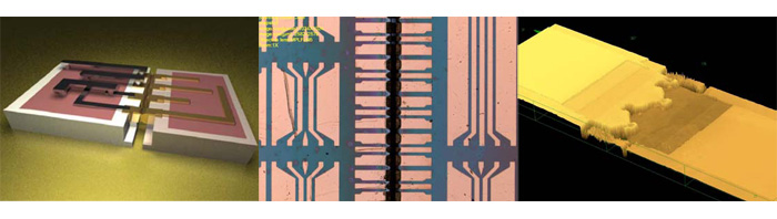
QP, which is based on established micro electro mechanical systems (MEMS)-inspired fabrication techniques, is fundamentally simple and practical. By providing contiguous chip-to-chip interconnections, it allows ICs to be tiled in two dimensions with gaps of only a few microns (μm) between each pair of chips. Each chip's sides have several short, conductive nodules that protrude horizontally to link directly to matching nodules on other ICs. The array of interconnected chips is called a quilt. The advantages of QP include reduced cost, weight and power dissipation, heterogeneous integration, high input/output (I/O) density, high bandwidth (no more than 0.1dB insertion loss caused by nodules up to 110 GHz[3]) and compatibility with current packaging technology and cooling schemes. At Notre Dame, I/O structures ranging from 10 μm to 100 μm wide have been fabricated (Figures 1-3).
Measuring etch depth: QP adds only a few additional steps to conventional IC manufacturing. First is to etch the nodule trench. At Notre Dame, the team usually uses silicon as the substrate. Deep reactive-ion etching (DRIE) is applied for the nodule trench etching; five minutes of DRIE yields nominally 20 μm-deep nodule trenches. Though the researchers at one time tried to use a stylus to measure trench depth, the tip diameter was too large to allow it to reach all the way into the trench. They have found that the OLS4100 measures the step profile of the nodule trench easily, accurately and quickly (Figure 4).
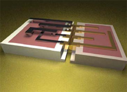 Figure 1: Rendering of QP interconnection, showing the edge nodules deposited deep into the substrate. |  Figure 2: One pair of assembled chips showing coplanar waveguides connecting them. |
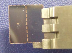 Figure 3: Quilt-packaged chips held on edge by tweezers, supported by the interconnected nodules. | 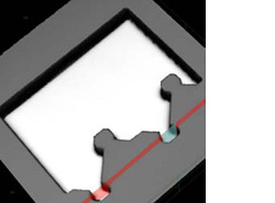 Figure 4: Step profile measurement for nodule trench etch step. |
Measuring surface roughness: After etching the nodule trench, copper is electroplated to fill the trench, and chemical-mechanical polishing (CMP) is applied to remove the overburden. After polishing, the abrasive particles, typically sub-micron silica or alumina in the polishing slurry, can adhere to the wafer surface and cause contamination. For RF devices, especially at high frequencies, high surface roughness can degrade the microwave performance. In fact, particulate matter on almost any semiconductor wafer can cause circuit defects and lead to yield loss in the final product. The OLS4100 provides a fast and accurate method to measure surface roughness, taking less than one minute to perform measurements that help ensure that the final product performs as expected (Figures 5a, 5b, 6).
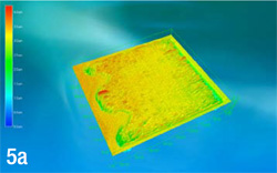 | 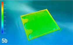 |
| Figure 5: Surface roughness measurements just after the CMP process. At (a), surface area texture measurement result just after the CMP process. At (b), the same measurement result after post-CMP cleaning. | |
| Surface Roughness Parameters | Before Post-CMP Cleaning | After Post-CMP Cleaning | |
| 44 nm | 13 nm | |
| Peak-to-Valley Roughness Rz | 243 nm | 87 nm | |
| 56 nm | 17 nm |
Figure 6: Laser confocal microscope data provides a comparison of surface roughness parameters before and after post-CMP cleaning.
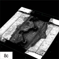
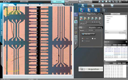 Figure 7: 2D image of assembled chips. | Measuring the vertical offset: After cleaning, chips are dry etched for separation and then assembled (Figure 7). But problems can arise in assembly if there is too much vertical offset between two chips' nodules. Extreme changes in contact area can adversely affect the electrical performance of the package. Therefore, care must be taken to monitor any vertical offsets between the nodules of various chips. With the OLS4100 microscope, team members obtain vertical offset and surface morphology information to help ensure that each "tile" is correctly aligned (Figures 8a-c, 9). |
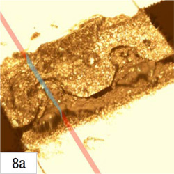 | 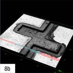 |
| Figure 8: At (a)-(c), 3D images for three different assembled nodule shapes. The offset for (a) is less than 1μm, and for (b) and (c) are about 7.3 μm. The stitching function of the LEXT OLS4100 makes it possible to create a high-resolution, widefield, 3D image. | |
 | 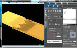 Figure 9: Widefield 3D view of assembled nodules shows the height difference of the on-chip interconnection metal layer and off-chip nodule interconnection from two chips. |
Accuracy and speed are vital
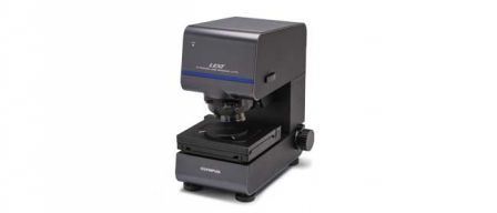
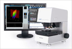 Figure 10: The Olympus LEXT OLS4100 Laser Scanning Confocal Microscope. |
The OLS4100 is used at several important process stages, not only because it provides 3D measuring capabilities and accurate surface roughness measurements, but because both types of data can be collected much more quickly than with other instruments, since the microscope captures images and performs measurements in seconds, where stylus-based systems require a probe to travel across a surface, which is much slower (Figure 10). The team discovered that the microscope system also
provides two additional benefits. First, it delivers much more accurate color imaging than any previous tool had offered. Even more important, it is very easy and convenient to use. While other laboratory measurement tools required extensive training, the Olympus system took only minutes to learn.
The process has already yielded extraordinary results. The Notre Dame research team is now working on developing methods to expand its utility and performance and make it more cost-effective to implement on a larger scale. A new company, Indiana Integrated Circuits, LLC, is commercializing QP technology for MEMS integration, RF systems, high-performance computing and other applications. |