Executive Summary
Quantitative information is central to the research and development efforts of flexible electronic devices. In this article, Dr Dario Gastaldi discusses how his research into the flexible conductive connection between electrical components, known as ‘the interconnect’, has benefited from in situ mechanical testing coupled to the quantitative imaging capabilities of the Olympus LEXT OLS4100. In this novel research, Dr Gastaldi’s group has generated quantitative evidence to support how interconnect geometry determines device integrity under strain. Such information facilitates numerical modelling systems for optimising the design process. The evolution of crack formation is also followed in more detail, while it has also been shown that plasma treatment of polymer can be detrimental to device strength under strain.
Introduction
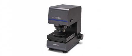
This article is the first of two case studies exploring the application of confocal laser scanning microscope with the Olympus LEXT OLS4100 is facilitating the different aspects involved in the development of flexible electronic devices. Electronic devices are becoming ever more innovative, with this rapidly evolving area holding the promise of flexible phones and wearable chemical sensors. While electronic sensor technology is well established for rigid devices, flexible devices must also overcome the challenge of maintaining electrical integrity during flexing and stretching. In the design of new devices, one approach to flexibility is to overlay rigid electronic components on a deformable substrate, linking these via conducting interconnects. Understanding how mechanical behavior evolves with strain is driving the development of this new technology, and a novel research approach is in situ testing, applying exact amounts of strain to a sample. When coupled with high-resolution imaging, this provides an accurate and detailed picture of how the device responds to strain, guiding the optimization of both the device materials and the fabrication process. A traditional observation technique for this is Scanning Electron Microscopy (SEM), however, light microscopy has now advanced to a stage where its capabilities are comparable to SEM. For example, confocal laser scanning microscopy (CLSM) also includes the added advantages of speed, ease of use and the ability to gather quantitative information. With its non-destructive 3D confocal laser scanning capabilities, the Olympus LEXT OLS4100 has proved its worth in advancing research into flexible electronics. This article explores the work of Dr Dario Gastaldi, whose group at the Politecnico di Milano (Milan, Italy) applies in situ testing of flexible electronic samples coupled to the LEXT OLS4100 for investigating and optimizing interconnect design (Figure 1).
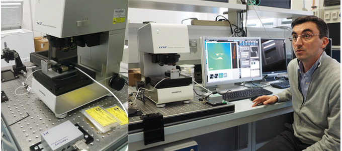
Figure 1: Micro-tensile testing machine coupled with the LEXT OLS4100.
The modular micro-tensile device fits on the stage of the LEXT, and strain is applied in 5% increments, with images acquired after each step.
Investigating the interconnect, in situ
In order for a flexible electronic device to function, the electronic components and deformable substrate must be connected. The interconnect must therefore be precisely engineered to remain attached to the substrate during complex deformation. “This can be achieved in different ways, with different materials and geometries [Figure 2],” as Dr Gastaldi explains. Through developing an in situ micro-tensile testing device coupled to high-resolution imaging, his group is working to understand and guide the two main features that have been found to affect adhesion between the interconnect and polymer substrate: geometric parameters and the fabrication process itself.
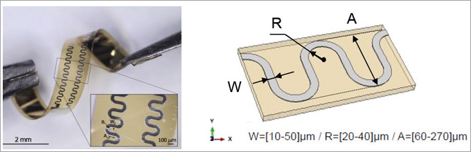 |
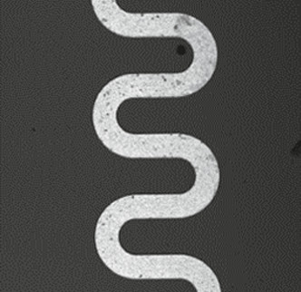
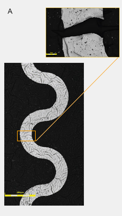
| Figure 2: Dr Gastaldi’s research looks at the interconnect design. The geometry of this meandering s-shaped interconnection is key for its mechanical-behavior, including width (W), radius (R) and amplitude (A). |
Optimizing interconnect geometry
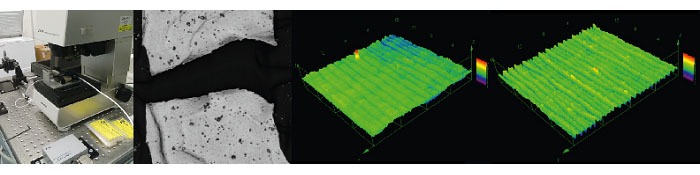
The differing interconnect geometries are defined by width, radius and length, and testing a variety of samples under mechanical strain provides insights into their differing mechanical behavior. SEM was previously employed with the in situ mechanical testing device, and although this technique has a resolution greater than CLSM, it fails to allow precise quantification of out-of-plane deformation. “This is exactly what we need, as we were not satisfied with a qualitative view,” says Dr Gastaldi. “Looking at the intensity image [Figure 3A, B], they are really very similar to the SEM. I was impressed by the image quality, not to mention the quantitative information.”
 W=50 μm R=40 μm A=270 μm No rotation of rectilinear arms: delamination-induced buckling →occurs at ~15% macroscopic strain →affects ~50% of bonded surface | 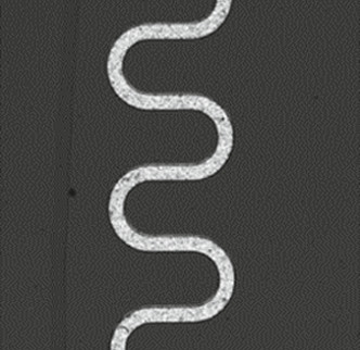 W = 10 μm R = 20 μm A= 90 μm Limited rotation of rectilinear arms: delamination-induced buckling →occurs at ~50% macroscopic strain →affects ~30% of bonded surface |
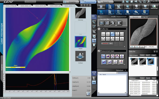
Figure 3: intensity images taken with the LEXT during the application of strain.
Comparing two distinct geometries of interconnect and their behavior under strain (A, B). Quantitative information on out-of-plane movement provides insights into behavior not available with SEM.
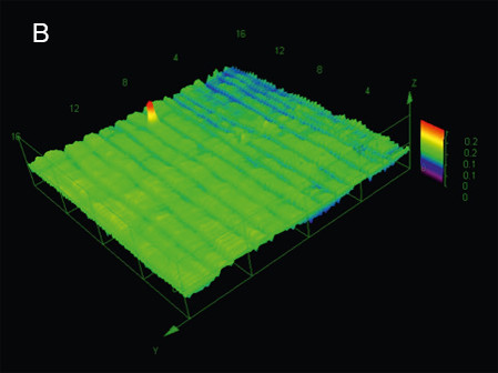
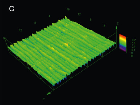
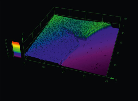 Figure 4: Crack development in the interconnect. The height map of the LEXT OLS4100 was visualized in 3D, showing the crack in the metallic interconnect above the polymer substrate. | The key parameter was found to be the length of the strut (or ‘amplitude’), and the LEXT OLS4100 also allowed the study of kinematics (geometry of motion) during mechanical testing to support this finding. Stretching causes compaction in the transverse direction, thus compacting the strut and leading to delamination due to buckling (Figure 4). Shorter struts exhibit less rotation (A versus B), as kinematic rotation can occur if metal delaminates from the substrate. Shorter struts are not prone to promote the buckling effect, and such a mechanical structure tends to accommodate much higher deformation. |
Quantitative modelling
Quantitative measurement is vital for the development of numerical modelling and therefore the design cycle, which consists of:
- Interconnect structural design
- Observation during mechanical tests
- Designing numerical models
- Simulate the same mechanical tests
- Feed the numerical model back into the design process.
Step number five utilizes the numerical model to guide the materials chosen based on mechanical properties or the geometrical design. “The height map function of the LEXT is the key to these measurements,” explains Dr Gastaldi, “and the quality of measuring a 3D structure with such accuracy exceeded expectations. Now we have the LEXT, we have not performed any SEM acquisition with our in situ mechanical testing device.”
Crack evolution
At specific strain values, the LEXT can also be applied to look at the cracking deformation of the interconnect in more detail. This cracking forms very close to the most delaminated areas, as metal alone is not able to sustain the same loading conditions as when adhered to the substrate, and starts to crack. This leads to a rise in electrical resistance, and the device fails. Dr Gastaldi explains: “With the LEXT, we can now observe this phenomena alongside the mechanical test. With SEM, however, we are not able to follow crack evolution, only broad measurements derived from the blurring during buckling, which is nothing comparable to the quantification of the LEXT.” CLSM was also found to be quicker compared to SEM especially in terms of sample preparation, as Dr Gastaldi goes on to say: “In half a day I have completed experiments that would have taken a week or longer with SEM. In some sense, SEM is a complementary observation to this, but for our purpose CLSM is a real step forward. The structural mechanical behavior of this tiny part is not only defined by the geometrical features, but also the adhesion properties between the metal and polymer.
Optimising adhesion between interconnect and substrate
The manufacturing process dictates the level of adhesion between the metallic interconnection and the polymer substrate. With this adhesion being central to functionality, optimum manufacturing guarantees maximum performance in terms of withstanding deformation. For example, in gold on Polydimethylsiloxane (PDMS) polymer samples, plasma treatment of the polymer surface is a standard technique employed to increase adhesion. “The plasma treatment permanently modifies the polymer, so the
question we want to ask is this – is the modified polymer compatible with deformation?” One side effect of the treatment is an increase in brittleness of the polymer, and Dr Gastaldi’s group has found this promotes superficial cracks and reduces the deformation that PDMS can sustain (Figure 5). However, the treatment protocol can be controlled through parameters such as energy and duration, and in situ mechanical testing with CLSM allows comparison between samples subjected to
varying treatments. As such, it is possible to identify the optimal plasma process, guaranteeing good adhesion without crack formation under a certain level of strain. Moreover, Dr Gastaldi’s work also found these cracks are present prior to the metallization process, confirming the brittleness derives from the plasma treatment alone (Figure 6). “With the LEXT, we have observed the cracks increase with strain, so we are now able to communicate this to our partners working on the
manufacturing technique. We have evidence to show that certain plasma treatments limit the mechanical strength of the device, and the metallization process is not the problem.”
 |  |
| |
| Figure 5: Crack formation in plasma treated PDMS. During 20% strain, the LEXT OLS4100 was used to visualize the PDMS layer following plasma treatment, prior to metallization. 3D analysis demonstrates extensive surface cracking in the interconnect (A). Cracks increase from 20% to 100% strain (B, C). | |
Summary
The work of Dr Gastaldi’s group focuses on optimizing the interconnect geometry and manufacturing process for flexible electronic devices. In situ mechanical testing provides insightful data of device behavior under strain. Combined with the quantitative information from the Olympus LEXT OLS4100, this approach has opened new avenues for modelling deformation and optimizing interconnect design. Quantitative evidence now supports how particular geometries with shorter ‘amplitude’ values are more resistant to delamination, facilitating the development of a numerical modelling system to enhance the design process. Quantitative information also allows the formation of cracks to be followed in more detail, while it has been shown that plasma treatment of polymers may increase adhesion, but promotes cracking at lower levels of strain. “The easy management of the LEXT allows us to focus our attention on our research,” comments Dr Gastaldi, whose group benefited from many features, including the height map and high lateral resolution. He affirms: “For those working with different types of mechanical testing, 3D profilometry is a really new, exciting aspect to this research. The LEXT provides us with a step forward, and now the question is how far can we go with this technique, and how can we couple the quantitative imaging capabilities of the LEXT with other techniques to drive the development of flexible electronics?”
Researcher Information
Dario Gastaldi and his colleagues are working at the department of Chemistry, Materials and Chemical
Engineering of the Politecnico di Milano, Italy investigating the mechanics of interconnects of deformable electronics. Email: dario.gastaldi@polimi.it