![]()
Manufacturing Printed Circuit Boards and Printed Wiring Boards
A printed circuit board (PCB) is a core unit of an electronic device with electronic parts mounted on a circuit board. The electronic parts conduct appropriate amounts of current or electric signals through the circuit pattern to make the electronic device operate. A printed wiring board (PWB), on the other hand, is a board with electronic parts in a circuit pattern that have not been mounted.
The PCB manufacturing process begins with a piece of copper foil. The foil is pasted on the plate of an insulator made of epoxy resin and glass. An agent called resist is then printed on the copper. Next, the copper portion surrounding the resist is removed using an agent—forming a circuit on a board.
In recent years, the use of multilayer circuit boards is becoming more common. This type of circuit board provides multi-functional electronic control with multiple layers of circuit boards.
An image of a multilayer circuit board
Although PCBs have controlled electronic devices for a long time, electronic device functionality has significantly evolved in recent years. As a result, improvements in their performance and quality is expected.
Consider this example: As the functions of smartphones, tablet PCs, and wearables grow, mounting parts in high density on a PCB is becoming essential. At the same time, hybrid electric and fully electric vehicles are growing in popularity. Now there are stronger expectations for circuit boards to accurately conduct large amounts of current to drive these vehicles. Not to mention, more products for automated driving of vehicles are available, such as an automotive millimeter-wave radar. This product produces radar waves from the circuit board. Innovations like this are attracting attention to new uses of circuit boards.
One of the technologies that supports these new electronic devices is higher precision of circuit shapes. Unless the circuit is formed with high precision to conduct the current or signal, the conduction will fail. This may prevent an electronic device from working correctly.
During the manufacturing process of PWBs, the shape of circuits is measured using an automated device that inspects the boards’ appearance. However, with large amounts of circuit boards to inspect, inspection time is limited, and automation can lead to oversights of defects.
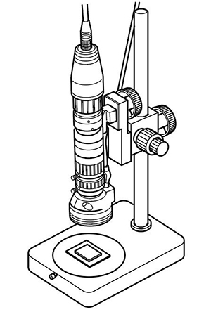
Therefore, a microscopic inspection is necessary to analyze circuit shape precisely. Some inspectors may turn to conventional digital microscopes to complete this task. However, these digital microscopes bring three main challenges for inspectors.
Challenges of Measuring Circuit Shape with a Conventional Digital Microscope
Low image resolution
Conventional digital microscopes typically offer one lens with a wide range of magnification using zoom. The problem is, image resolution decreases as magnification increases. This leads to a blurred image, presenting a challenge when measuring circuit shape. Often inspectors need to see multiple types of circuit shapes on the same printed wiring board. With a conventional digital microscope, you cannot achieve a clear image of all circuit shapes.
Complex lens replacement
While conventional digital microscopes have high-magnification lenses, many models only include one lens. As a result, anytime you switch magnification you must replace the current lens. This is a time-consuming process when measuring circuit shape, since it requires you to find the circuit focus position all over again.
Unreliable measurement values
Most digital microscope manufacturers do not guarantee measurement accuracy and precision. Without a guarantee of the circuit shape measurement value, the data is unreliable.
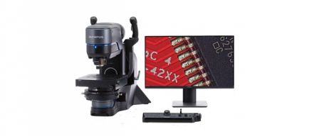
Advantages of Measuring Circuit Shape with the DSX1000 Digital Microscope
High-resolution objective lenses achieve clear images
The DSX1000 digital microscope is equipped with high-resolution objective lenses. Zooming in to a high magnification leads to a high-resolution image, which you cannot achieve with conventional digital microscopes. The high-resolution images allow you to accurately measure the circuit shapes of PWBs.
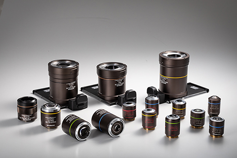
DSX1000 objective lenses
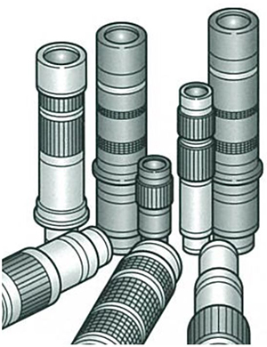
Quick-change lenses provide flexibility
Changing magnification with quick-change lenses is a simple and fast process. You can instantly switch from a low magnification to a high one (or vice versa) without needing to search for the focus position again. With a large selection of easy-to-change lenses, you can measure with the optimal objective lens for the circuit shape size.
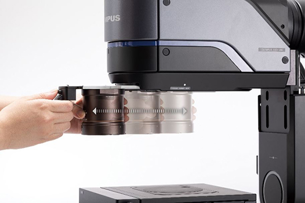
Quick-change lenses
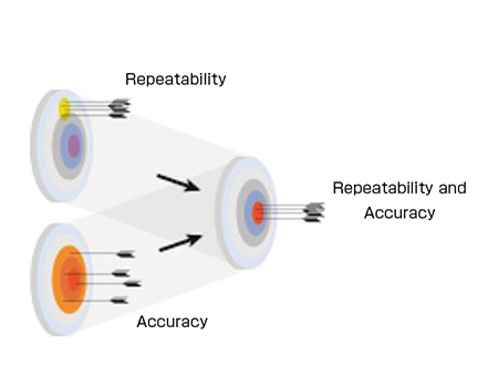
Guaranteed accuracy and repeatability
With the DSX1000 digital microscope, accuracy and repeatability are guaranteed for all magnifications*. Increased measurement reliability enables you to present results to external parties with confidence.
*To guarantee XY accuracy, the calibration must be performed by an Olympus service technician.
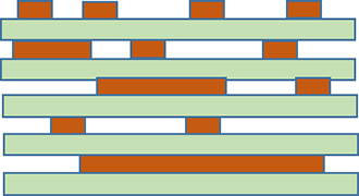
Images
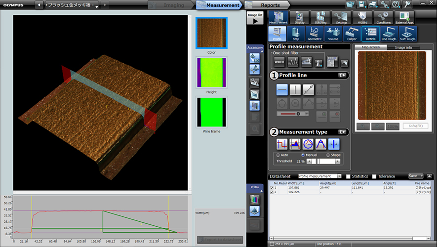
The circuit shape of a printed wiring board captured using the DSX1000.