Application
A lead frame is an important part that serves as a base for integrated circuit (IC) and large-scale integration (LSI) semiconductor packaging. The frame is a thin layer of metal that supports a semiconductor chip to connect it to outside wiring. The frame is comprised of a die pad that holds the chip, inner lead wires that connect to the chip, and outer lead wires. The inner leads are connected to the chip with gold wiring. The surface of the inner leads must be rough to ensure that the gold wire and inner lead join together adequately. Consequently, checking surface roughness is an important part of quality management.
As semiconductor packages become smaller and denser, the inner leads also become smaller. Manufacturers must employ tools that enable them to measure and evaluate surface roughness in a very small area.
The Olympus solution
Olympus' LEXT 3D scanning laser microscope enables high-resolution surface roughness measurement with a horizontal resolution of 0.12 μm and a step resolution of 5 nm. With traditional contact-type roughness measurement tools, placing the stylus directly on a single ultra-fine lead is very difficult. The LEXT’s non-contact laser microscope can image an ultra-fine lead for measurement without damaging the sample surface. The microscope’s confocal optical system captures 3D visual data over small steps.
Inner lead
Objective lens 10X | Inner lead in 3D
Objective lens 20X |
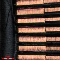

Surface roughness of the tip of an inner lead

Objective lens 100X, Zoom 2X