Microscope Solutions for
PCB Manufacturing
- Home
- Microscope Solutions for PCB Manufacturing
- Making the Inner Layer
Making the Inner Layer
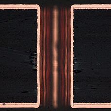
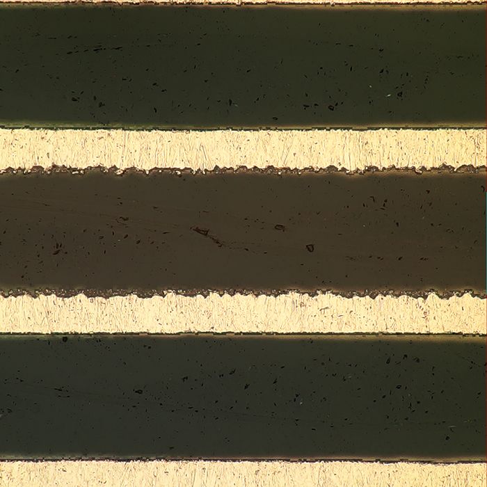
After applying a resist to the copper foil, the surface is etched to form a circuit. This process is repeated many times to complete the inner layer board where the circuit is formed.
Measuring the Dimensions after Etching
Inspectors must determine the dimensions of the inner layer surface after etching to help ensure proper electric transmission.
Our Solution
Our DSX1000 digital microscope can acquire 3D images and provide dimension measurements, enabling you to analyze the surface dimensions of the inner layer.
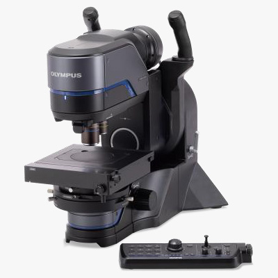 DSX series digital microscope | 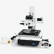 STM series measuring microscope | 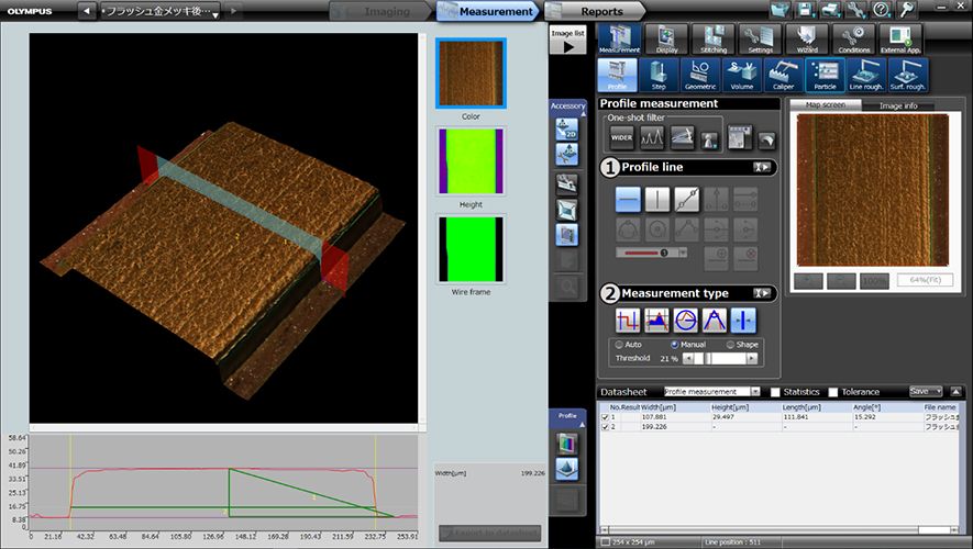 3D dimensions of a PCB |
Application Notes
Explore related applications:
 |
| ||
 |
| ||
 |
|
DSX series digital microscope Request a Quote | STM series measuring microscope Request a Quote |
Not available in your country.
Not available in your country.