ElFys, a pioneering company founded by researchers from Aalto University in Finland, has been at the forefront of developing light sensing technology into high-performance photodiode products used across industries.
Here we explore the brilliance of ElFys' photodiode technology and the vital role our DSX1000 digital microscope plays in the pursuit of excellence within their production process.
Keeping Technology Close to the Heart
Have you ever wondered how your smartwatch can accurately detect your heartbeat? How does a small piece of metal on your wrist manage to capture the subtle variations in your heart rate throughout the day?
The answer lies in a remarkable technology known as the photodiode, a light sensor that can convert light into energy. The smartwatch emits a green light onto your skin, which your red blood cells absorb. As your heart beats, your blood vessels expand and contract rhythmically, causing fluctuations in the intensity of the reflected light. The photodiode can measure these changes in reflected light, enabling your smartwatch to calculate your heart rate in real time.
But photodiodes' brilliance extends far beyond smartwatches. These versatile devices can be found in an array of everyday gadgets, including laptops, mobile phones, cars, and even rings. Their application spans far and wide, ranging from airport luggage scanners and medical imaging devices in hospitals to cash registers at retail stores.
Sensing Potential: The Start of ElFys
Founded by a team of researchers from Aalto University in 2017, ElFys is at the forefront of cutting-edge photodiode technology, revolutionizing light sensors with an inventive combination of modern micro-electromechanical systems (MEMS) nanotechnology and atomic layer deposition (ALD).
With this innovative technology, ElFys can capture every single ray of light, leading to improved performance for a huge array of devices that rely on light sensors. The company’s dedication to excellence and commitment to research have made it a leading provider of high-performance photodiode products in a diverse range of industries.
The technology behind ElFys' photodiodes revolves around three innovative techniques: front surface nanostructuring, conformal ALD alumina deposition, and an induced junction. This unique combination creates a highly efficient photodiode with superior light absorption and the capacity to capture the entire charge produced, granting unmatched light-sensing capabilities.
Choosing the Right Tool for the Job
In the pursuit of excellence, ElFys relies on advanced inspection equipment to help ensure the quality and precision of its photodiode products. This includes using microscopy to detect any defects on the wafers, chips, and packaged components.
When it came to choosing a microscope for this role, ElFys looked for an instrument that offered exceptional flexibility, capable of accommodating various types of samples rather than being limited to a single specific purpose.
During our conversation with ElFys Founder and CEO Mikko Juntunen and Project Manager Juha Heinonen, they shared valuable insights into their decision-making process behind choosing the DSX1000 microscope.
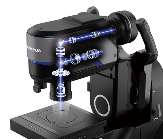
The DSX1000 digital microscope
Mikko commented, “After reaching out to inquire about potential solutions, we were fortunate to discover that the Finnish distributor, GWB, had a demo unit available right here in Finland. This presented us with a fantastic opportunity to get hands-on experience with the product before making any decisions.
Visiting GWB, we were able to test the DSX1000 digital microscope using our own samples, witnessing firsthand how it operates. This hands-on experience was crucial in our decision-making process, as it enabled us to truly understand its capabilities.
In contrast, other manufacturers typically only provide data sheets outlining the tool's features, leaving us uncertain about its actual performance. The ability to try the tool ourselves gave us unparalleled confidence in its suitability for our needs. We knew that it could fulfill our specific requirements thanks to the practical experience we gained through testing.”
The Pursuit of Excellence
“As you can see from the color of my hair, I've been in the field for quite some time, and when I think of a microscope, it is an Olympus.” — Mikko Juntunen, the founder and CEO of ElFys
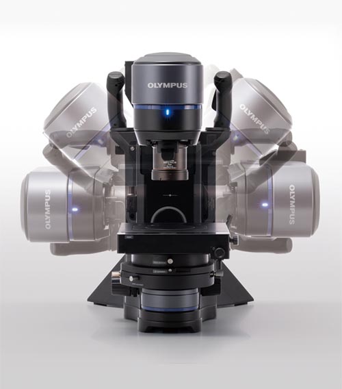
The DSX1000 digital microscope
The DSX1000 digital microscope has become an indispensable tool for ElFys, facilitating detailed inspections of silicon wafers, chips, and packaged components after production. Given the small size of semiconductor components, ElFys manufactures them on 6-inch-wide wafers, about the size of a CD, with thousands of components within each wafer.
In terms of workflow, the first step involves inspecting the wafer for defects and abnormalities in the chips. The microscope's darkfield mode has proven particularly helpful in highlighting scratches and defects, helping ensure that only the highest quality products reach the market. ElFys also noted the extremely useful seamless stitching capability of the microscope, which played a crucial role in inspecting the entire wafer. Due to the size of the wafer, it needed to be inspected in quarters. However, with the seamless stitching feature, the microscope enabled the creation of large, high-quality images.
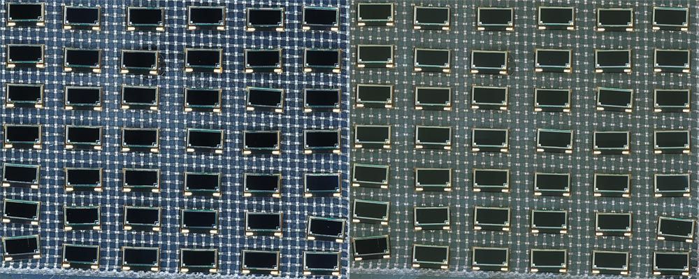
Stitched image in darkfield (left) and MIX illumination (right) of a surface-mount component.
Captured by Juha Heinonen using the DSX1000 digital microscope. Images courtesy of ElFys.
One specific challenge faced by ElFys was inspecting chips coated with a transparent epoxy layer. Here, the microscope's differential interference contrast (DIC) mode proved invaluable, revealing scratches and microstructures on the epoxy surface.
Once the initial checks are completed, inspection of the photodiode package—which plays a critical role in allowing light to reach the most sensitive part of the device—is necessary. At this point, the structure goes from 2D to 3D, making the microscope's ability to perform 3D imaging instrumental in inspecting the packaged components. The ability to capture 3D images offers a comprehensive view of complex structures, simultaneously bringing different levels of depth into focus and providing detailed insight into the assembly.
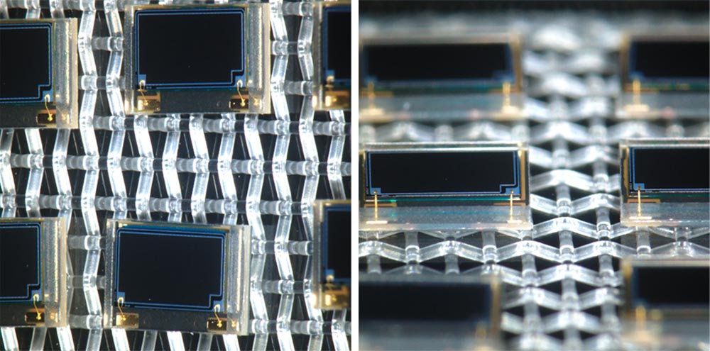
Darkfield images of a surface-mount component from different angles. Captured by Juha Heinonen using the DSX1000 digital microscope. Images courtesy of ElFys.
When asked about recommending the DSX1000 digital microscope to other businesses in the industry, Juha was emphatic: "The DSX1000 digital microscope is an excellent option, especially when dealing with smaller samples that can easily fit on the stage. Its high flexibility allows for a wide range of observation modes, enabling multiple angles to be explored. The user experience is intuitive and efficient, saving valuable time by eliminating the need to fine-tune settings.
In fields such as semiconductor research, where numerous similar samples require examination, this tool proves invaluable. Its automation and fast imaging capabilities allow researchers to quickly analyze multiple samples, maximizing productivity and efficiency. With this level of automation and speed, researchers can focus on studying a greater number of samples in a shorter period, significantly enhancing their workflow."
Future Directions
ElFys continues to push the boundaries of light sensing technology, with ongoing research aimed at extending the capability of their photodetectors into the deeper infrared spectrum. By using different semiconductor materials, ElFys aims to overcome the limitations of silicon and achieve relevant responses in the near-infrared range, catering to industries such as wearable health technology, where additional parameters such as blood glucose or lactate levels are of interest.
As a company driven by research and innovation, ElFys has emerged as a pioneer in the field of light sensing technology. The company’s commitment to excellence and diversity, combined with a strong team of researchers and engineering leaders, has propelled them to the forefront of the industry. With the DSX1000 digital microscope as a vital ally in their pursuit of excellence, ElFys continues to shape the future of light sensing
applications across various sectors, contributing to a brighter world.
Related Content
Digital vs. Optical Microscopes: An In-Depth Comparison
Detecting Manufacturing Defects on Semiconductor Wafers Using a Digital Microscope
Controlling Quality Control in Electronics Manufacturing Using PRECiV™ Software