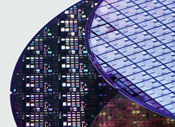

Residue and defects on silicon wafers stand out : Our novel MIX illumination combines brightfield, darkfield, simple polarized, and fluorescent lighting techniques to reveal defects that are otherwise difficult to see.
Sample  Semiconductor Wafer |
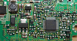
Improved contrast : A combination of hardware and software remove glare and halation, improving the contrast of your images. Even highly reflective components are now easily visible.
Sample  Printed Circuit Board(PCB) |
Fits 6-inch wafers and large printed circuit boards : The large stage has a flat top design, enabling larger samples to extend off the edge. The stage’s long stroke can cover 150 mm x 100 mm inspection area.
Not available in your country.
Not available in your country.