Silicon carbide (SiC) is an important material in the semiconductor industry, as it is used for its technical and physical properties in modern circuits. SiC devices are revolutionizing power electronics across industries, offering increased efficiency, power density, and reliability in applications such as electric vehicles, renewable energy systems, and industrial drives.
Here we highlight how EEMCO, a manufacturer of SiC materials, streamlined its image analysis process for completed etched SiC wafers through a collaboration with Evident. As a result of this work, our custom software with machine learning capabilities has improved the accuracy and efficiency of defect detection and characterization on wafers. Learn more about this innovation and its impact across industries.
SiC Device Applications
Three key applications of SiC devices are in the automotive, high-power electronics, and renewable energy industries.
1. Automotive
The demand for electric drives in automotive vehicles has been increasing rapidly. With a market share of more than 60%, electric drives are a significant factor in the market for high-power electronic devices.1 This has created an increasing demand for highly efficient power semiconductors for use in electric/hybrid vehicles (EV/HEV).
This application immediately suggests the use of SiC-based power semiconductors, as they have clear advantages over conventional Si-based components. The higher efficiency and power density provided by SiC lead to increased ranges, smaller system dimensions, and faster charging times. Typical applications include highly efficient inverters, on-board charging electronics, boosters, and DC/DC converters.
One of the essential criteria for the economical use of SiC single crystals is the lowest possible defect density in a single crystal paired with the largest possible crystal wafer (a 6 in. wafer is now standard, with 8 in. wafers soon to be introduced). This requires the mastery of complex crystal growing technology, such as that provided by EEMCO.
2. High-Power Electronics
A wide range of industrial applications are driven by the need for auxiliary power supplies. These applications typically include motor drives, inverters, and industrial manufacturing equipment (including robotics).
With its unique properties, silicon carbide strongly supports improvement in the energy efficiency, reliability, and performance of these systems.5 Typical devices using SiC-based technology range from Schottky diodes (also called Schottky barrier diodes, or SBDs) to junction-gate field-effect transistors (JFETs) and metal-oxide semiconductor field-effect transistors (MOSFETs).
In fact, SiC SBDs are widely used in insulated gate bipolar transistor (IGBT) power modules and power factor correction (PFC) circuits. SiC does not just increase efficiency and reduce cooling requirements in these applications. It also simplifies device design, in that it reduces the amount of passive components and enables simpler designs—without sacrificing performance. These characteristics are also useful in the IT industry, particularly in data centers.
3. Renewable Energy
Solar power, wind power, and renewable energy storage are industries that display remarkable growth. The renewable energy sector is one that is effectively and efficiently balancing supply and demand. While renewable energy has been a favored application for SiC products for many years, the current climate and energy crises have increased the demand for alternative energy sources even more.
Common applications involve high-efficiency electronic power devices such as inverters and boosters (power converters), as well as essential components for power conversion and energy storage systems. The typical charging losses for such devices range between 6 and 9%, figures that can be reduced dramatically by applying SiC technology.1 SiC-based device technology also reduces the need for complex circuit designs, requiring fewer overall components.
Controlling and Monitoring the Final Product Quality of SiC Wafers
With the need for SiC-based device technology in many industries, SiC manufacturers are focusing on innovation, quality, and efficiency in their production process. One example is EBNER EUROPEAN MONO CRYSTAL OPERATION (EEMCO), a startup spun off from EBNER in 2020.
"EEMCO is the first independent company in Europe aiming to mass manufacture 200 mm SiC substrates for the semiconductor industry," explains Mirko Löhmann, responsible for process engineering at EEMCO.
Leveraging its 12 years of R&D experience in crystal growth equipment design and manufacture, the Austrian company develops dedicated furnaces for the 4H SiC single crystal growth process and is taking the next step with 200 mm boules and pucks.
At their Leonding, Austria, facility, EEMCO's team of international experts cultivates SiC single crystals for the semiconductor industry.
"These crystals are used in high-power applications, particularly in the automotive, industrial, and renewable energy sectors," says Sebastian Hofer, who oversees defect engineering at EEMCO.
EEMCO operates a growing number of furnaces where SiC single crystals grow using a physical vapor transport (PVT) process, forming a single crystal within an SiC vapor phase.
"Our goals are to manufacture strategic, high-tech products as the first independent European company producing these types of SiC crystals, offering a high-quality alternative to dependence on suppliers in the USA or China," says Hofer. Löhmann adds, "As a sustainable and energy-saving product, SiC also significantly contributes to CO2 reduction across various markets and consumer end products."
Specializing in high-quality 150 and 200 mm pucks, EEMCO leverages proprietary furnaces and process technology. "Over the past two years, we've filed over 30 patents related to SiC crystal growth equipment and processes. Our strategy is to grow 150 and 200 mm SiC single crystals for global ingot manufacturing and supply, with a primary focus on European customers," explains Hofer.
To control and monitor the production process and final product quality, a 100% optical analysis of the entire 150 or 200 mm diameter SiC wafer is required. This presents two challenges:
- High-resolution imaging: Acquiring high-resolution images (1-2 μm/pixel) of the entire wafer takes time and generates gigabytes of data per wafer.
- Dislocation detection: Traditional particle analysis is insufficient for detecting clustered and overlapping dislocations. Simple threshold-based segmentation lacks accuracy for meaningful results.
"We need to acquire and analyze complete etched SiC wafers," says Löhmann. "We collaborated with the Customized Solutions team at the Evident Technology Center Europe (ETCE) to develop a solution based on PRECiV™ software, the Evident industrial imaging platform we use in our labs," he continues. This collaboration uses machine learning to improve defect characterization on complete etched SiC wafers.
Designing a Custom Solution for Optical Analysis of Large SiC Wafers
Dr. Norbert Radomski and Dr. Sergej Bock, solution managers in the Customized Solutions Group (CSG) of the Evident Technology Center Europe (ETCE), explain the advantages of this customized wafer inspection solution.
“With the acquisition and analysis of complete etched SiC wafers, we have increased our portfolio of wafer inspection solutions.2, 3 Now we can acquire and analyze complete 6 in. and 8 in. etched silicon carbide wafers,” says Norbert. Sergej adds, “The solution uses machine learning to improve defect characterization. In addition, the analysis is performed in parallel with the data acquisition to improve efficiency.”
This inspection solution is important to identify and characterize defects that may occur during the SiC crystal growth process.
SiC crystals are grown using the physical vapor transport (PVT) method, where a single crystal is grown in an SiC vapor phase. Controlling the crystal stress during the growth process is key to minimizing extended densities of defects, such as micropipes (MP), basal plane dislocations (BPD), threading screw dislocations (TSD), and threading edge dislocations (TED).4 These defects affect the electrical properties of the SiC wafer. The molten KOH etching method is considered an effective method to characterize dislocations in SiC.5
As an example, Figure 1 shows various types of defects on an etched SiC wafer, such as micropipes (MP) basal plane dislocations, threading screw dislocations (TSD), and threading edge dislocations (TED).
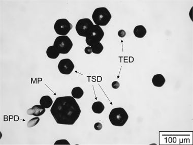
Figure 1. Microscope image of typical defects on an SiC wafer etched with KOH.6 Image source: MDPI.
The request from EEMCO given to Evident: To control and monitor the production process and the quality of the final product, a 100% optical analysis of the complete 6 in. or 8 in. diameter SiC wafer must be performed.
This is quite a challenge, says Norbert: “First, one needs high-resolution images (1–2 µm/pixel) of the whole wafer, which occupies time and generates gigabytes (GB) of data per wafer. Secondly, the detection of dislocations cannot be performed with classical particle analysis. The dislocations tend to cluster and overlap, so simple threshold-based segmentation is not accurate enough to provide meaningful results.“
Thresholding does not detect specific structures in the images. Instead, it detects multiple objects at once without distinguishing between them7, based on the predefined grayscale or RGB intensity values. Sergej notes, “In contrast, machine learning forms rules for object detection based on multiple examples of representatives of objects of interest.” Automated evaluation, based on deep artificial neural networks that have learned to classify image areas independently of previously set threshold values in the image, makes image analysis easier and more accurate.7
The Custom Solutions team demonstrated that a segmentation approach using an appropriately trained neural network (see Figure 2) can be used to automatically separate clustered and superimposed dislocations (see Figure 3), resulting in sufficient defect density analysis.
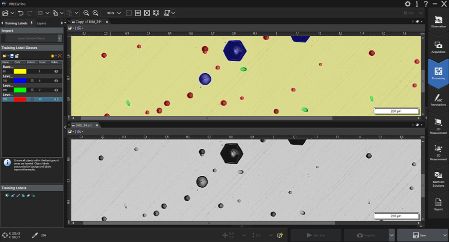
Figure 2. Screenshot of dislocation training labels (upper part) and a brightfield image of an etched SiC wafer (image resolution: 1.095 µm/pixel).
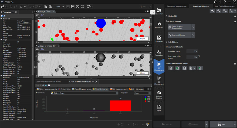
Figure 3. Screenshot of detected dislocations yielded by neural network segmentation (upper part) and a brightfield image of an etched SiC wafer (image resolution: 1.095 µm/pixel). Note that clustered and overlayed dislocations are separated.
However, it should be noted that both training a neural network and executing a neural network require a lot of computing power, which is usually provided by hundreds or thousands of Compute Unified Device Architecture (CUDA) cores of a CUDA-enabled NVIDIA graphics card.
“A total image of a 6 in. wafer imaged with a resolution of 1.095 µm/pixel consists of approximately 4,000 single images and is about 25 GB in size. Calculating a segmentation by a neural network on the whole image would take hours even with a state-of-the-art graphics card,” explains Sergej.
Therefore, as the quality criterion of an SiC wafer is the density of dislocations per area, the approach of the custom solution is to split the process into an acquisition and an analysis method using two PCs for parallel working. This doubles the throughput, improving efficiency.
Norbert explains the overall custom solution: “The image of the whole wafer captured by the acquisition system is stored in a predefined location. A status file indicates whether the image is complete and can be analyzed with the neural network-based defect wafer analysis solution. With the wafer analysis solution, the large wafer image is divided into smaller tile images with definable dimensions, and a batch analysis process with neural network segmentation is applied to each tile. The calculation on the smaller tiles improves efficiency. The result also provides a dislocation density number per individual tile area. Since the positions of the tiles on the wafer are known, the output is basically a density map of the entire wafer.”
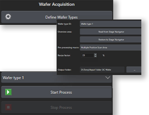
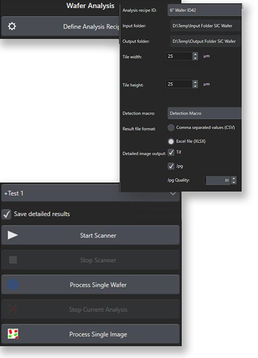
Now let’s take a look at the custom solution workflow, which begins with wafer acquisition (see Figure 4).
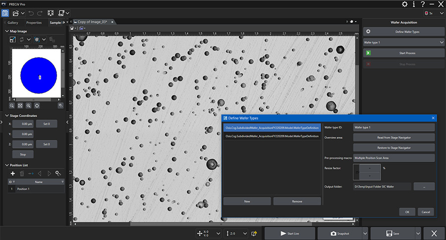
Figure 4. Screenshot of the wafer acquisition solution showing the process definition dialog for Define Wafer Types.
Below are the steps to acquire a large panorama image of the entire SiC wafer (see Figure 5). The resulting image file (our proprietary VSI format) is then used in the analysis workflow.
SiC Wafer Acquisition Workflow
Figure 5. Custom acquisition workflow for SiC wafer inspection. | Define Wafer Types:
Drop Down List: Select predefined acquisition recipes from the wafer type ID.Start Process: Starts the predefined acquisition process. An input dialog opens to set the product ID and measurement count (will be incremented automatically). The software then automatically calculates the tilted plane Z-correction based on the Z-values of three stage positions. The Z-values are determined by the autofocus.
Stop Scanner: Stop the acquisition process. |
With the wafer analysis solution, the large wafer image is divided into smaller tile images and a predefined macro (here, the Count and Measure solution with neural network segmentation) is applied in a batch process on every tile (see Figure 6).
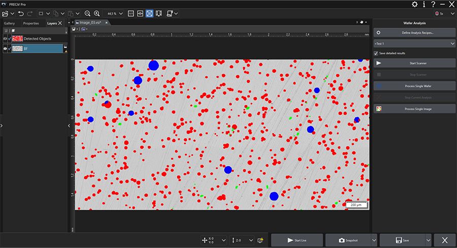
Figure 6. Screenshot of the wafer analysis solution showing the process definition dialog for Define Analysis Recipes.
SiC Wafer Analysis Workflow
Figure 7. Custom analysis workflow for SiC wafer inspection. | Define Analysis Recipes:
Drop Down List: Select predefined analysis recipes.Start Scanner: Check the input folder for VSI files with the associated status file indicating the image status as acquired (ready for processing). Start the batch process (crop image into sub-tiles and perform the analysis).Stop Scanner: Stop the scanner function.Process Single Wafer: Select a single VSI image for processing.Stop Current Analysis: Stop the running analysis.
Process Single Image: Select a single TIF image for processing. |
SiC Wafer Inspection Results
The results can be exported as a CSV or XLSX file to provide data per tile with individual information on the detected defects (Figure 8, top image) or as a summary table with defect classes per tile (Figure 8, bottom image). This first sheet includes one image per tile, along with the object IDs (identified defects) and their center of mass in the X-direction, center of mass in the Y-direction, and various description values for their shapes, such as sphericity and orientation.
The summary file shows the row and column IDs of all the sub-tiles and the individual defect counts per class. Each class represents a specific defect type (see Figure 1 for examples). Lastly, the software provides an overview image of the SiC wafer (Figure 9) as a TIF with a detection layer showing a color code for the class per defect. For documentation purposes, a compressed JPEG image with burned-in detection overlays is also an option. Together, these organized images and data enable
efficient analysis of defects on the entire wafer.
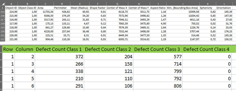
Figure 8. SiC wafer inspection results exported as a CSV or XLSX file provide details on the defects, including their count per class, their shape, and other parameters.
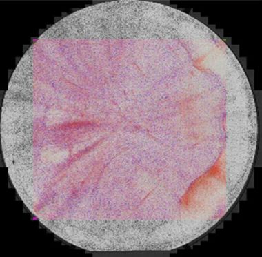
Figure 9. Overview image of the entire SiC wafer.
Conclusion
The collaboration between EEMCO and Evident in streamlining image acquisition and analysis processes for etched SiC wafers underscores our commitment to innovation and quality in SiC manufacturing. Through custom software and machine learning, defect characterization on SiC wafers has been significantly improved, paving the way for enhanced product quality and performance across diverse applications. As the demand for SiC-based devices continues to grow, such collaborative efforts exemplify the industry's dedication to meeting evolving technological challenges and driving forward the era of sustainable, high-performance electronics.
References
- “EEMCO Applications.” 2021. EEMCO.
- Bock S. and Radomski N. 2022. “Optimizing Wafer Inspection with Advanced Microscopy and Image Analysis.” Electronics Today.
- Bock S. 2023 “Optimize Your Wafer Inspection Microscope and Workflow.” Evident InSight Blog.
- Seldrum T. “Short Overview Etch Pits: High Quality 150 mm SiC Substrates for Power Electronics Application.” Power Electronics Europe. Issue 4.
- Wang et al. 2021. “Micropipes in SiC Single Crystal Observed by Molten KOH Etching” Materials. 14(19), 5890.
- Ou et al. 2023 “Novel Photonic Applications of Silicon Carbide.” Materials. 16(3), 1014.
- Janovsky A. 2023. “The Potential of AI-Based Image Analysis in Metallography and Materialography.” Evident InSight Blog.