6. Application Examples
The laser scanning microscope is used in many markets. Typical application examples are shown in the table below.
Semiconductors
Electrode substrate for electrostatic mirror array
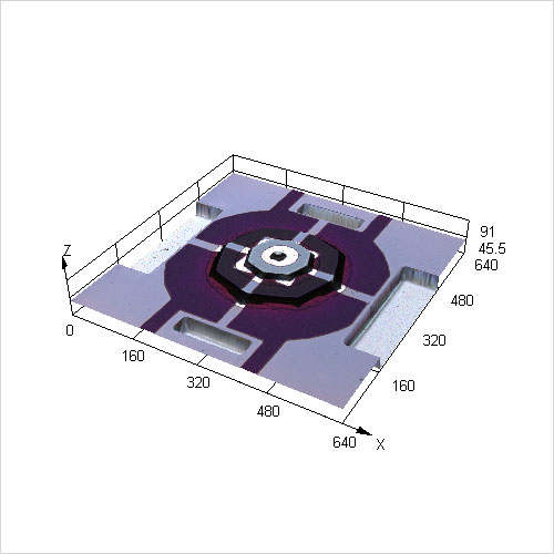 | The performance of a device such as MEMS often changes depending on its shape. Therefore, shape measurement is an important control item. Laser scanning microscopes can accurately acquire the three-dimensional shape of a device and measure steps or other shapes. |
Microlens
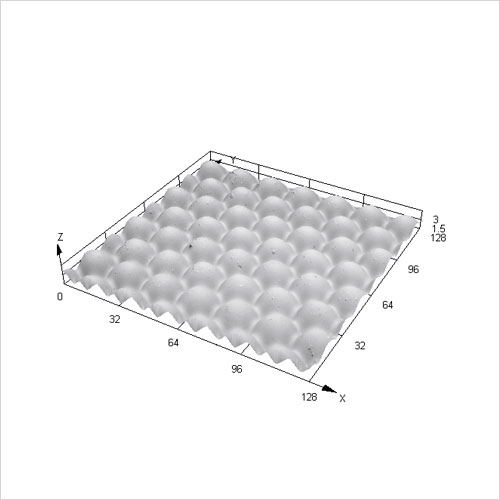 | Laser scanning microscopes can acquire the shape of a transparent body if the sample surface has a reflectance of several percent. This sample is a microlens with a diameter of 20 μm and a height of 10 μm. |
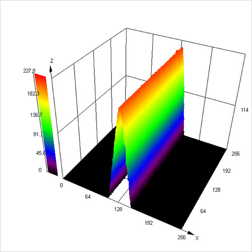
Wafer bump
 | The size of the wafer bump in high-density packages is continually getting smaller. Typical control items are the bump height, diameter, and bump pitch measurement, though the bump volume, surface roughness of the vertex of the bump, and other items are also being monitored recently. The figure shows the test pattern of a soldered wafer bump with a diameter of 12 μm and height of 3 μm. |
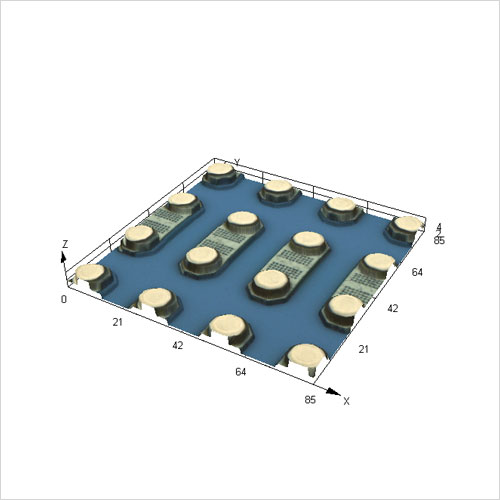
Electronic components
CCD
 | The OLS5000 has an optical microscope function that acquires color information and can add color information to the acquired three-dimensional information before display. |
Resin part on a PCB board
 | The OLS5000 is used to manage the width of minute copper wiring on PCB boards and is sometimes used to evaluate the sectional area of copper wiring to evaluate the resistance value of the copper wiring. The surface roughness of the pad section where CSP bumps are soldered is also evaluated. In addition, recent board roughening technology has improved the adhesion and conductivity of copper foil. Laser scanning microscopes are increasingly implemented for the evaluation of this technology. |
Connector section on a flexible board
 | The connector section is important for maintaining the reliability of electronics using flexible boards. The shape and depth of dents, which become the latches for connectors, and the depth of the groove generated when actually connected are accurately measured. |
Materials
Optical waveguide prism
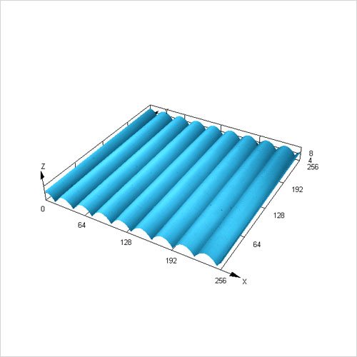 | Conventional optical measuring units have a shortcoming in that the reflectance of slopes is low and the area around the wall surface of a sample is difficult to see. With the OLS5000, the ability to detect steep slopes is dramatically improved and the shape of a steep slope on an optical waveguide prism can be acquired. |
Frosted glass
 | The OLS5000 can acquire the shape of a transparent sample if the sample surface has a reflectance of several percent. Because the OLS5000 can acquire three-dimensional information and measure surface roughness, the roughness of different kinds of frosted glasses under different sandblast conditions can be evaluated and controlled. |
Adhesive tape
 | In the past, stylus-type roughness measuring units scraped the surface when scanning a soft sample. The laser scanning microscope, which enables noncontact measurement, can measure the profile regardless of the condition of a sample surface such as its viscosity, elasticity, and softness. |
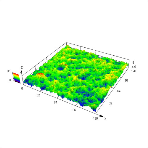
Carbon
 | The OLS5000 can acquire data if the sample surface has a reflectance of several percent. Therefore, the surface status of a black sample with low reflectance such as carbon can be clearly observed. |
Automobile parts
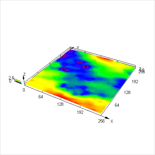
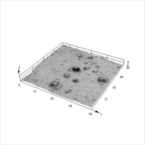
Foreign object on a filter
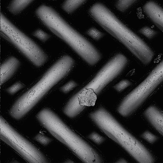 | Because the laser scanning microscope can acquire an image that keeps the whole sample in focus, even a sample with large irregularities can be observed and evaluated as a whole. This sample shows a foreign object left on a filter. The width of the foreign object is about 30 μm. |
Mechanical processing
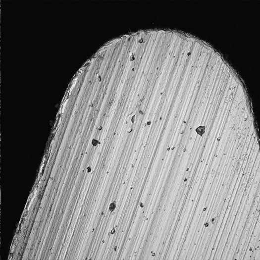
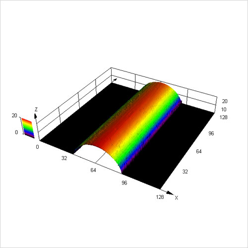
Tip of razor blade
 | Conventional optical measuring units have a shortcoming in that the reflectance of slopes is low and the area around the wall surface of a sample is difficult to see. With the OLS5000, the ability to detect steep slopes is dramatically improved and the shape can be measured at 85°. |
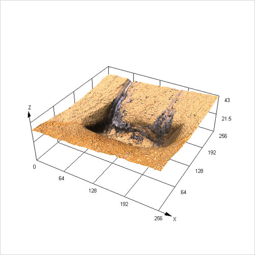
Metal cutting/grinding face
 | The smallest radius of the laser spot in the OLS5000 is about 0.2 μm. Therefore, the OLS5000 can accurately acquire data from minute deep grooves that the stylus of a stylus roughness gauge cannot enter. |
Chips of tool bit not used
 | Laser scanning microscopes have better plane-resolving power than optical microscopes and can acquire images that keep the whole sample in focus. Therefore, cracks, wear, or other damage on minute chips of tool bit can be observed. |
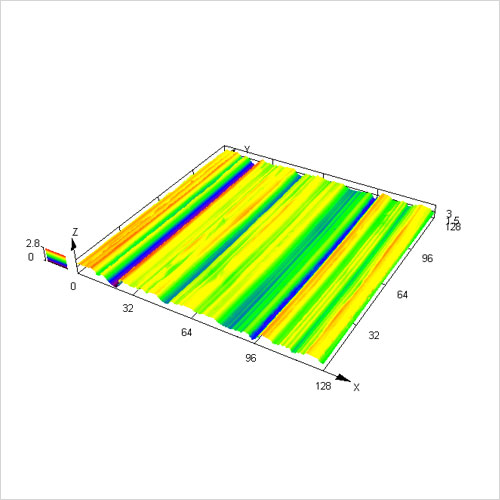
Extra-fine wire
 | While wires with a diameter of a few dozen microns are difficult to scan with a stylus-type roughness measuring unit, the laser scanning microscope facilitates positioning in such minute areas, allowing users to easily measure surface roughness. |
Miscellaneous
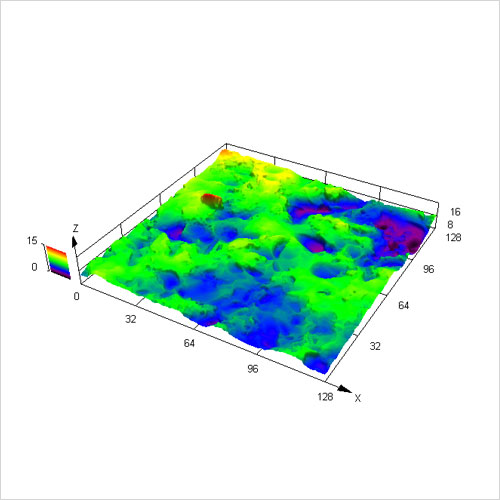
Surface of tooth
 | Laser scanning microscopes can acquire three-dimensional data as long as the material has some reflection. Therefore, laser scanning microscopes are used to observe various samples such as hair, teeth, and skin in addition to industrial products. |
| Others | |
| Semiconductors |
LSI/IC
LD/LED MEMS Bare wafers Photomasks Resist Bump Thin films Microlens |
| Electronic components |
FPD
Organic EL Packages Wire-bonding FCB Die-bonding PC boards Lead frames LD/LED PSS Crystal oscillators Capacitors HDD Motors Optical fibers |
| Materials |
Iron and steel
Nonferrous metal Fiber Coating Paint Adhesive agents Film Resin materials Ceramic Cloth Paper Plates Rubber Tonner Magnets Glass |
| Automobile parts |
Pistons and cylinders
Sensors |
| Mechanical processing |
Blades
Tip tools End mills Abrasive cloth Tool bits Gears Screws Molds Injection molding Grind stones |
| Mechanical devices |
Injection needles
Surgical knives Catheters Implants Stents Endoscopes Artificial hearts Artificial bones |
| Energy |
Solar batteries
Lithium-ion batteries |
| Research |
Universities
Public research institutes Private research institutes |
| Miscellaneous |
Cosmetics
Hair Skin Red blood cells Pills Emulsion Paper money Coins |
Conclusion
The application range of the laser scanning microscope for three-dimensional measurement targeting minute objects is expected to grow by leveraging the features of the confocal microscope and adding new functions to the software. It is also expected that users will require an even higher level of accuracy and resolving power from the device.
References
- Hirohisa Fujimoto: Outline of Nano-material Engineering Vol. 1 (Edited by Kazuyuki Hirao, et al.), pp. 604–612, FUJITECHNOSYSTEM, 2005.
- Kentaro Yamazaki: O plus E, 26(8): pp. 901–906, 2004.
- Shigeru Nishida: Science and Engineering of Materials, 40(5): pp. 220–224, 2003.
- H. Miyajima, et al: Journal of Microlectromechanical Systems, 12(3): pp. 243–251, 2003.
- Hirohumi Miyamoto, Takefumi Ito: The Tribology, 19(7): pp. 30–33, 2005.
- Chikara Nagano: Latest Optical Technology Handbook (Edited by Junpei Tsujiuchi, et al.), pp. 685–705, Asakura Publishing, 2002.
- 1. Basic Principles of Laser Scanning Microscopes
- 2. Resolving Power of Laser Scanning Microscopes
- 3. Measurement Accuracy of Laser Scanning Microscopes
- 4. Software for Laser Scanning Microscopes
- 5. Basic Features of Olympus Industrial Laser Scanning Microscopes
- 6. Application Examples
> Click here for detail about OLS5000, laser confocal microscopes
> Click here for detail about OLS4500, nano search microscopes