Process improves inspection efficiency, increases yields, and improves process control
Cadmium zinc telluride (CdZnTe), or CZT, is a compound semiconductor of cadmium, zinc, and tellurium. It is used in a variety of applications, including radiation detectors, substrates for MgCdTe (IR detectors), photorefractive gratings, electro-optic modulators, solar cells, and terahertz generation and detection. The band gap (energy difference) varies from approximately 1.4 to 2.2 eV, depending on composition.
After dicing and polishing CZT, manufacturers of these devices require the ability to image through samples using IR technology, a microscopic imaging technique that utilizes light wavelengths between 1100 and 1200 nm and imaging sensors to capture the reflected light wavelengths and create an image.
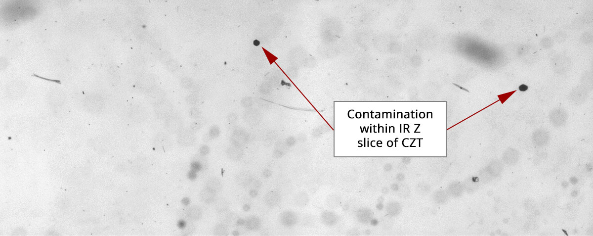
Following image acquisition, one common task is to determine the location with the least amount of secondary phases, shown as particles, within the CZT over an entire sample area. Placing the circuitry or conductive point on the location with the least amount of secondary phases improves the performance of the detector, solar cell, or photorefractive gratings. The lower the percentage of secondary phases present, the less diffraction of signal passing through the CZT. Following the automated image analysis, the system needs to drive to the location with the lowest percentage of particles in order to place a laser mark around the area for cut-out. Currently, most of this type of work is done manually and is time-consuming due to the large area of inspection. Automating this type of inspection process would improve the manufacturer’s efficiency of inspection, increase yields, and improve process control, saving them both time and money.
Automating the Process with Advanced Image Analysis Software
Advanced image analysis software—in combination with a compound or wafer inspection microscope and a high-sensitivity digital camera—can automatically scan through CZT and detect secondary phases to determine the location of the area with the lowest percentage within a predetermined size range. Furthermore, this system can return to this area to perform a more sensitive scan and place a mark using an attached laser marking system.
The optimum system configuration includes:
- OLYMPUS Stream® image analysis software
- Olympus BX53/61 upright compound microscope or Olympus MX51/61 wafer inspection microscope, including reflected and transmitted light IR
- Olympus high-sensitivity XM10IR digital camera for imaging within the IR bandwidth
- X, Y, Z motorized components connected directly to PC for software control
- Laser marking system attached to the reflected light illuminator for marking the sample surface to define the cut-out area
The most significant advantages of the configuration are saving time and reducing cost, while increasing accuracy. This is attributed to scan automation, as opposed to a manual configuration. Scan automation is made possible by X, Y, and Z automated stitching, which enables the user to look through the entire surface area using one seamlessly stitched image made up of many different scans. This enables easy detection of image spots that may point to material defects. Increased yields and the ability to pinpoint areas for process improvements are additional advantages.
 |
Get In Touch