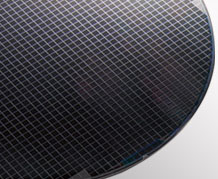
Photoresist image
Measuring the Thickness of a Photoresist Film
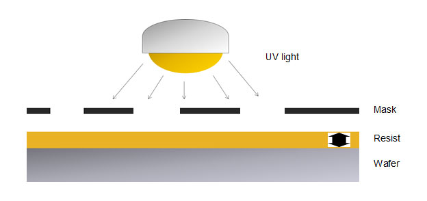
During the semiconductor manufacturing process, design patterns are printed on a silicon wafer using a technique called photolithography. To ensure that this pattern is accurate, the thickness of the photoresist film must be carefully managed. However, measuring the thickness can be challenging because of light reflected from the silicon beneath the resist.
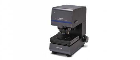
Olympus’ Solution: Thickness Measurement Using the OLS5000 Microscope
Measuring the thickness of photoresist film using the Olympus LEXT OLS5000 3D laser scanning microscope is quick and easy due to its unique features:
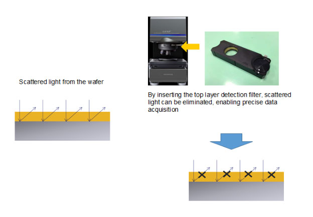
Using the microscope’s top layer detection filter, scattered light from the silicon can be eliminated, even for transparent photoresist film, enabling proper thickness measurements.
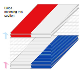
The skip scan function enables the microscope to scan only the area that is necessary for data acquisition, helping to significantly speed up the scan speed. For example, a resist with a thickness of 23 µm can be scanned in as little as 10 seconds.