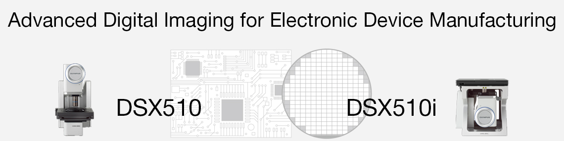
See the Details
Get clear images at high magnification with no complicated sample preparation.
1100x magnification
Sample: IC patterns on a semiconductor wafer
See the fine IC patterns and tiny defects on a wafer with sharp detail.
【Sample Application】 
Semiconductor bear wafer lasermark
See more |
| Observed sample 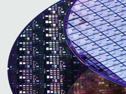
Semiconductor wafer |
|
|
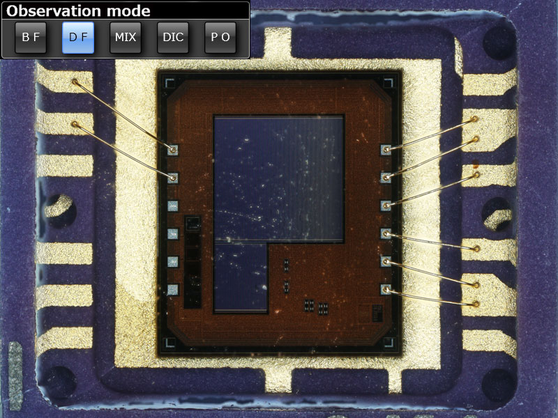
Switch Observation Techniques with One Click
With a single click, you can change between five observation methods for maximum flexibility.
Darkfield observation
Sample: An IC chip on a UV sensor
Observe metal parts such as bonding wires and lead frames.
Brightfield observation
Sample: An IC chip on a UV sensor
The IC chip's pattern can be observed with a crisp image.
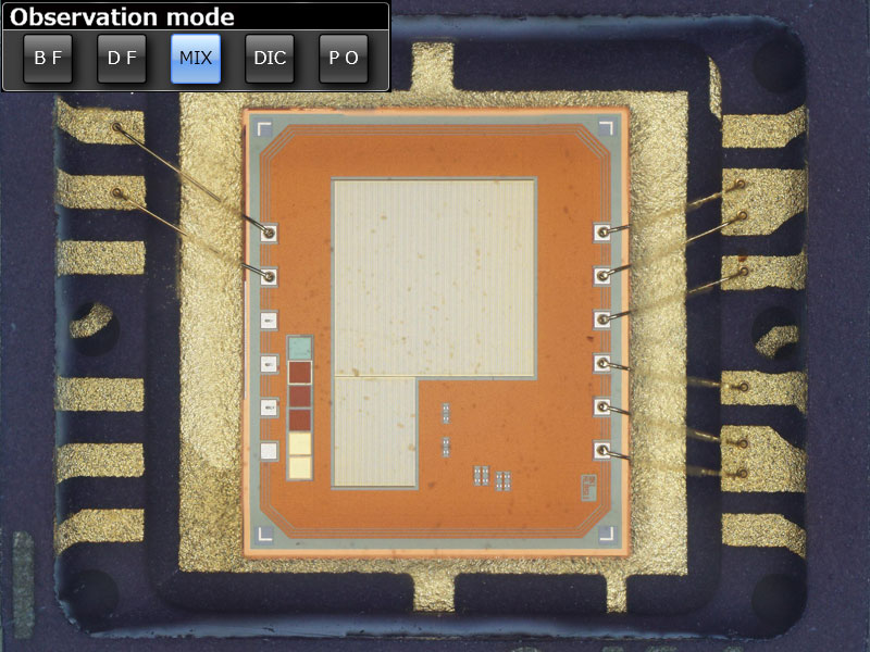
MIX observation (darkfield + brightfield)
Sample: An IC chip on a UV sensor
The IC chip and metal parts can be viewed at the same time by combining brightfield and darkfield images.
【Sample Application】 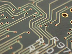
Contaminants in Printed circuit board through-holes
See more |
| Observed sample 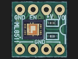
UV sensor |
|
|
3D Images
View your sample in three dimensions from any angle.
|
Sample: pins on a printed circuit board
View the shape of projecting pins in 3D.
|
【Sample Application】 
Detecting flaws in heat-treated aluminum alloy parts
See more |
| Observed sample 
Printed circuit board |
|
|
Measure Complex Shapes in Real Time
Using 3D measurement, a DSX microscope can instantly measure complex shapes and points that are difficult to approach.
|
Sample: MEMS
Small gaps on the MEMS can be measured from any direction in real time.
|
【Sample Application】 
Sectioning analysis for ball grid array
See more |
| Observed sample 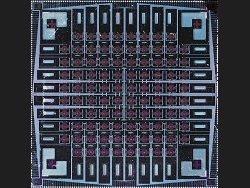
MEMS |
|
|
Not available in your country.
Not available in your country.
Redirecting
You are being redirected to our local site.
Lo sentimos, la página solicitada no se encuentra disponible en su país.

.jpg?rev=9FB6)