Background
Wafer-level CSP (Chip Size Package) is a technique of packaging an integrated circuit at wafer level. CSP facilitates high-density mounting without wire bonding. In the case of wafer-level CSP, a wafer goes through several semiconductor manufacturing processes, including forming electrode terminals, attaching solder balls, and resin encapsulation. The package then undergoes dicing so that its size is as small as a wafer chip. This technique has two key features: 1) it allows high-integration semiconductor devices to be mounted on a printed board with a small footprint and 2) packages made using this technique are less vulnerable to damage compared to those made using the ordinary CSP technique.
Increasingly, the wafer-level CSP technique is being used in more applications including smartphones, digital cameras, digital audio players, laptop PCs, and watches. As electronic devices continue to get smaller and manufacturers seek to further control the shape of device surfaces and solder balls, wafer-level CSP will continue to gain importance. Consequently, the size and shape of essential wafer-level CSP components such as wafer bumps, solder balls, and copper posts have to be precisely measured to ensure that electronic devices function properly (Figures 1 and 2).
The Olympus solutions
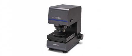
The Olympus LEXT 3D measurement microscope enables you to make non-contact, high-resolution 3D measurements of the shape and surface roughness of wafer-level CSPs. The exceptional optical capabilities of the microscope combined with powerful software for measuring and detecting irregularities without damaging the device facilitates easy CSP inspection.
Features of the product
The Olympus LEXT makes 3D microshape, non-contact measurements of electrical components. The microscope features ultra-high-resolution combined with high pixel density to ensure accuracy. The LEXT’s high inclination sensitivity is excellent for measuring complex and steep-sided component parts.
Image
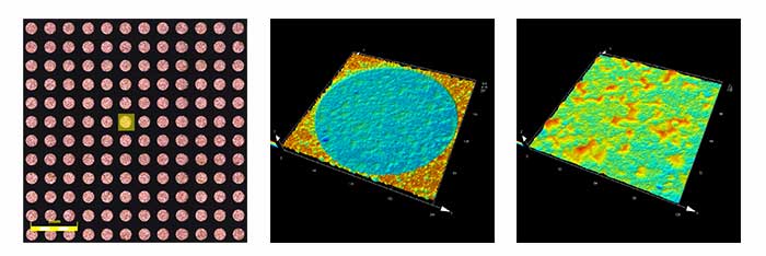
Figure 1: High resolution images of the top surface of a copper post on an integrated circuit
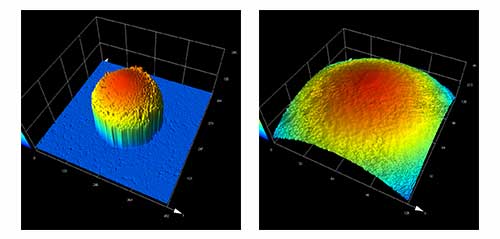
Figure 2: 3D measurement analysis of a solder ball