Nicknamed the mother of electronic products, printed circuit boards (PCBs) are critical to modern electronic devices in just about every industry. A key step in manufacturing PCBs is bonding copper foil to a dielectric resin substrate. Before bonding, the copper surface is intentionally roughened to improve its ability to bond with the dielectric material. However, rough copper foils cause a loss in conductivity, which can negatively impact how the circuit board functions. In addition, conductor loss significantly increases as the current frequency increases due to what’s known as the skin effect. In high-frequency 5G electronics, this can be a problem.
What Is the Skin Effect?
The skin effect is the tendency of a high-frequency alternating current to flow through the conductor’s outer layer, or skin. The higher the current’s density (or frequency), the closer it flows to the surface. High-frequency currents flowing near the surface lead to a smaller skin depth. When the skin depth corresponding to the circuit’s operating frequency is lower than or equal to the copper foil surface roughness, the signal propagates on the copper foil surface.
Since 5G technology uses a current frequency higher than 4G or 3G, its skin depth is lower, and its current density is higher. However, rough surfaces can negatively affect the current’s transmission path. The rougher the copper foil’s surface is, the longer the signal transmission path and the greater the conductor loss. We can’t use perfectly smooth copper foil because some roughness is required to bond the foil to the substrate, so copper foil roughness must be carefully controlled—it should be rough enough to adhere well to the substrate but smooth enough to minimize transmission loss.
Surface Roughness Testing
The conventional method for measuring surface roughness uses a stylus that is dragged across the sample’s surface. However, the stylus can damage sensitive surfaces—like copper foil—and your measurement data is limited by the diameter of the stylus tip.
Laser scanning confocal microscopes are preferred tools for roughness measurement because they offer many advantages over conventional measurement methods.
4 Advantages of Laser Microscopes for Measuring Surface Roughness
No contact required
As their name implies, laser microscopes use laser light to collect data, so nothing physical touches the sample. This eliminates the problem of scratching or damaging your sample during testing using a stylus. A laser microscope also has the advantage of being able to make accurate roughness measurements no matter the sample’s surface condition.
|
|
|
.jpg?rev=7D27)
-update2.jpg?rev=48E2)
Finer roughness measurement data
A conventional stylus’s tip radius is only about 2 to 10 μm, making it difficult for it to capture roughness data at the microscopic level. The laser on our OLS5100 laser scanning microscope has a radius of only 0.2 μm, so it can capture much finer surface roughness data that a stylus cannot measure.
|
|
|
.jpg?rev=D63E)
.jpg?rev=D63E)
Comprehensive sample information
A stylus can obtain only one type of information—roughness. In contrast, our laser microscope can simultaneously obtain three types of information—laser images, color images, and 3D feature data. Combining these data can give you a better understanding of the surface roughness.
|
|
|
.jpg?rev=DD8C)
-update.jpg?rev=DD8C)
Automated inspections
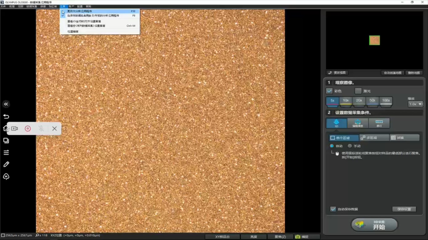
Another advantage of laser confocal microscope’s is the ability to automate part of the inspection workflow, improving reproducibility and minimizing operator-to-operator variability. For copper foil roughness measurement, the OLS5100 laser microscope ca n automate the inspection workflow from data acquisition to report creation. Just press the Start button, and you can perform fine profile measurements at the sub-micron level.
To make the device even smarter, the microscope software’s macro function enables a computer to control a range of microscope operations so that you can test and analyze samples quickly and accurately.
Related Content
Surface Roughness Measurement: Practical Tips to Get Started
On-Demand Webinar: Roughness Parameters—How to Select the Most Meaningful One?
Roughness Measurement with the LEXT Laser Scanning Microscope
Get In Touch