Space is at a premium in the lab, so a system that can perform as several microscopes in one is essential. Today’s digital microscopes do just that, offering a magnification range that’s capable of producing a field of view of 22 mm down to 42 µm. This ‘macro to micro’ capability makes it easy to observe samples under low magnification to view features in context before inspecting a small area under high magnification to see the details. Combined with a user-friendly interface, even a novice is capable of quickly and easily achieving results using just one instrument.
Macro
The capabilities of digital microscopes extend beyond just a wide magnification range—adding motorized components to the microscope extends the system’s functionality even further. For larger samples that extend beyond your system’s field of view, you can quickly and easily capture images of the entire sample using the
Micro
Staying on the same microscope system and moving to a higher magnification, it’s possible to move to any point on the sample just by clicking on the macro image, eliminating the need to re-find defects if you were to switch from one system to another or having to rely on complicated coordinate methods. Whether you’re interested in examining surface roughness, micron-sized defects, structural features, or something else, our digital microscopes come equipped with a range of conventional optical techniques and advanced image processing capabilities, such as high dynamic range (HDR), to enhance surfaces and contrast.
One example of a type of inspection that’s often challenging for conventional microscopes but digital microscopes excel at is working with polished samples. On upright microscopes, polished samples are often disregarded since they’re usually not perfectly planar and horizontal, making it difficult to level the sample so that its surface is at a right angle to the microscope’s optical access. Consequently, inverted microscopes, where the sample naturally lies at a right angle to the axis of the microscope, is preferred. However, when using digital technology and motorized components, it’s possible to compensate for the limitations of upright microscopes, opening up the possibilities for additional fields of analysis.
Advanced analysis
Integrating digital microscopes with advanced image analysis software further enables you to customize the instrument. Using standard operating procedures and the guided operation functions available in our DSX series digital microscopes, doing your work is easier than ever. Now, even users with relatively little training can engage in many types of analyses, from grains analysis to sophisticated particle classification.
Check out these examples showing how a single digital microscope system can tell the whole story.
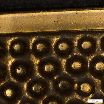 A macro image of an aluminum badge. The round features are bumps. | 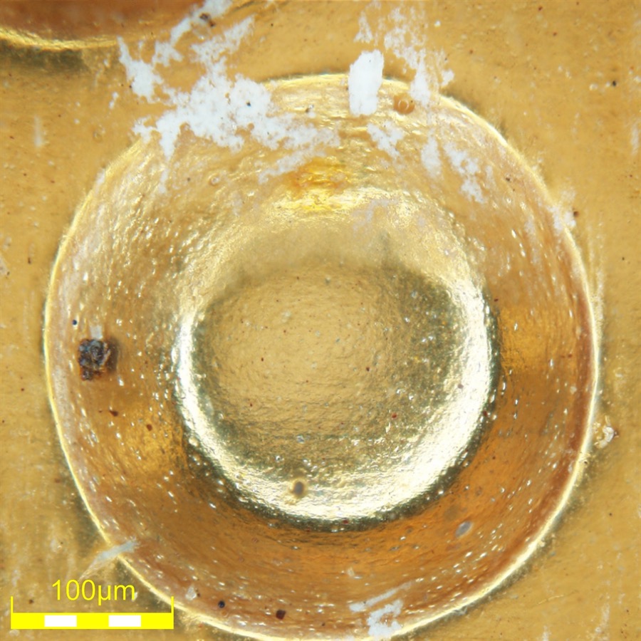 Looking more closely at one of the bumps. |
 An image of the bumps surface taken at 5000x magnification. | 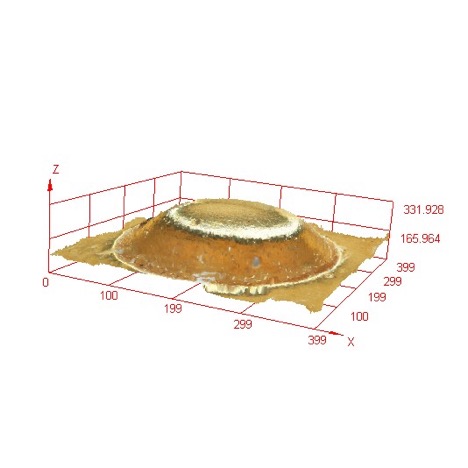 A 3D map of one of the bumps. |
Related Content
Digital Microscope Application: Edge Analysis of Semiconductor Chip Dicing
Digital Microscope Application: Fracture Surface Analysis
Digital Microscope Application: Inspection of Chipped Gears
Get In Touch