Background
As electronic equipment continues to become smaller and more sophisticated, the demand for miniaturized printed circuit boards (PCBs) is increasing. An essential part of manufacturing PCBs is binding copper foil to a dielectric resin substrate. To ensure that the copper foil adheres securely, the resin surface is roughened to increase the surface area. If the surface is too rough, it creates electrical impedance that negatively impacts the electronic device. Consequently, surface roughness must be measured to make sure it remains within optimum limits.
The Olympus solutions
The Olympus LEXT 3D measuring laser microscope is engineered to measure surface roughness with a planar resolution of 0.12 μm and an unevenness resolution of 5 nm, which are ideal for PCB roughness applications. The microscope features both high pixel density and high inclination sensitivity enabling you to measure surfaces with fine irregularities and steep angles. The LEXT employs non-contact roughness measurement technology so a substrate’s surface is protected from being damaged.
Features of the product
The LEXT features ultra-high-resolution images with high pixel density for accurate 3D observations. The microscope has high inclination sensitivity and reliably measures samples with steep angles. Surface roughness measurements are non-contact so the resin substrate is protected. The LEXT supports JIS/ISO surface roughness measurement requirements.
Image
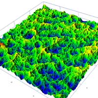
Figure 1: A 3D image showing the roughness measurement of a resin substrate