Introduction
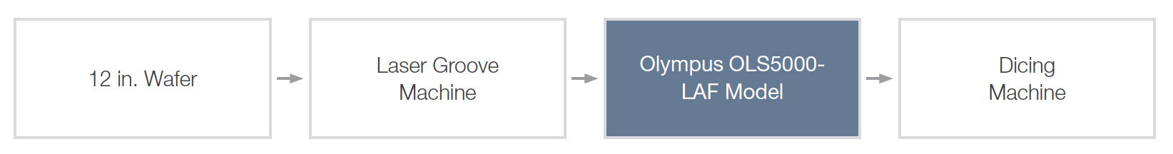
In the semiconductor integrated circuit manufacturing process, a silicon wafer is diced to separate it into individual dies that are then assembled onto lead frames and encapsulated into electronic chips.
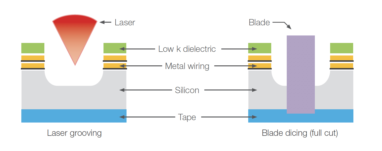
The conventional dicing process uses a very sharp blade to cut through the silicon wafer to separate the dies. However, blade dicing is problematic. In particular, the blade can stress the dies and wafer as a whole no matter how sharp it is. The need to achieve increasingly smaller and thinner dies and the migration to low-k dielectric and copper materials have necessitated the addition of laser surface grooving prior to the blade dicing process to overcome topside delamination and sub-surface cracking of the dielectric material.
Laser grooving is a two-step process. First, a laser is used to isolate the edge of the die by creating ‘train track’ grooves through the wafer’s surface layers and just into the silicon layer. Next, subsequent laser passes remove the material in the ‘street’ between the train tracks. Once the streets have been cleared, the wafer is diced with a blade. Thanks to this laser grooving process, the blade only has to cut through the silicon and not any of the surface materials.
Measuring the Profile of Laser Grooves Using a Laser Confocal Microscope
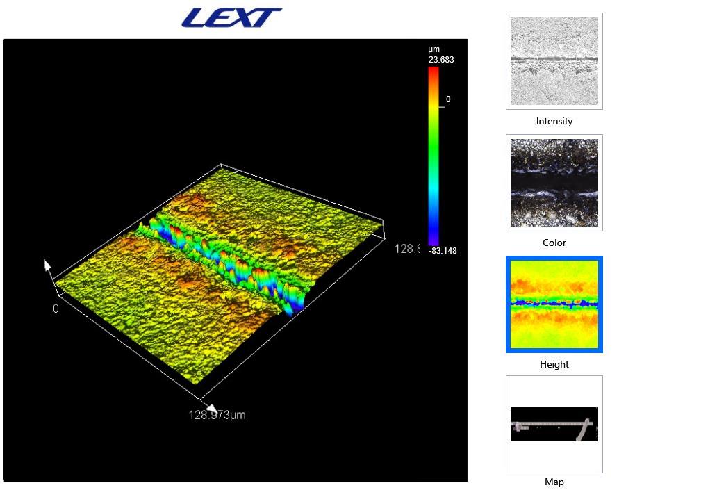
The advantages of laser grooving have made it the preferred semiconductor manufacturing process for wafer dicing. However, laser grooving also has its own challenges. The laser system is complex, and it needs to be accurately positioned over the wafer to ensure that it creates grooves along the correct profile on the die streets. The groove itself must be extremely precise and conform to the profile and tolerance set by the manufacturer. To help ensure that their laser system is set up correctly, manufacturers need a tool that enables them to measure the profile of the laser grooves to check whether they meet the specified tolerance.
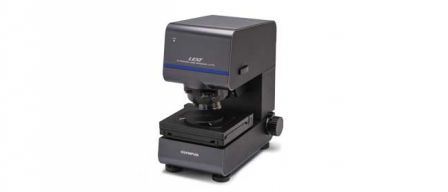
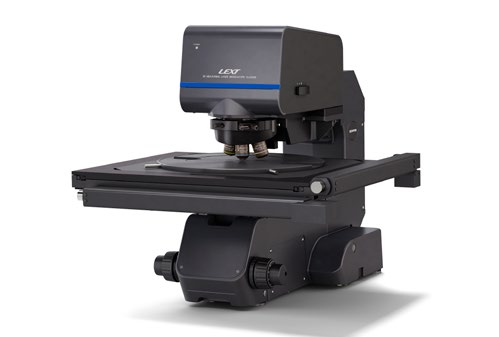
The Olympus OLS5000 laser scanning confocal microscope is well suited to provide accurate profile measurements of laser grooves. It can provide the quantitative data required to check that the grooves meet manufacturer tolerance standards. The microscope offers fast, precise imaging and a large 300 mm × 300 mm (roughly 12 in. x 12 in.) motorized stage that readily accommodates 12-inch wafers. The microscope software’s acquisition and analysis functions make it simple for operators to measure the depth and width of laser groove profiles.
Advantages of Using the OLS5000 Microscope for Laser Grooving Quality Assurance
- The microscope offers fast, precise imaging and a large 300 mm × 300 mm (roughly 12 in. x 12 in.) motorized stage movement that readily accommodates 12-inch wafers.
- Programmable multi-area acquisition feature enables automatic multipoint acquisition of laser grooves on a wafer.
- The combination of the microscope’s 405 nm laser source, 0.8 nm optical z scale, 4K scanning technology, and dedicated LEXT™ objective lenses provide accurate 3D profiling of laser grooves during the acquisition process.
- Users can create an analysis template for automatic measurement of the width and depth of laser groove 3D profiles.
- All of the measurement data can easily be complied into a single, comprehensive quality report.
 | 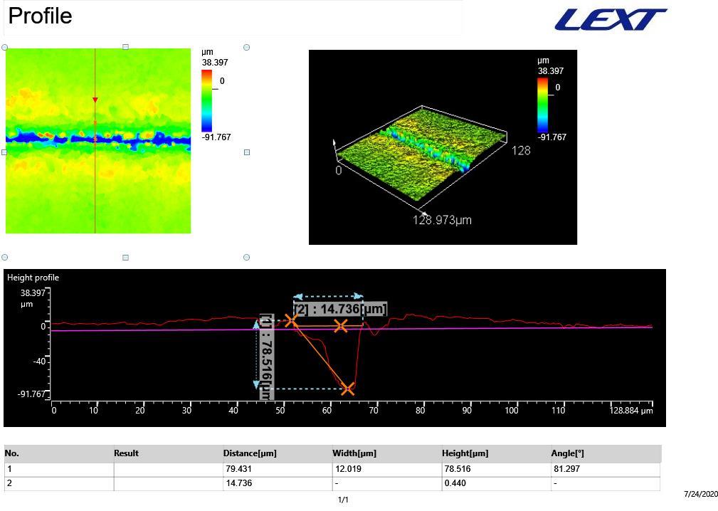 |
| Laser groove profile measurements |