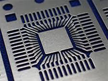
Lead frame die pad
Inspecting Lead Frame Die Pad Roughness
During semiconductor manufacturing, a diced integrated circuit (IC) chip is picked up and mounted on the die pad of a lead frame. Before the IC chip is finally mounted, an adhesive (die bond paste) is applied to the die pad. Either a conductive or non-conductive die bond paste is used, depending on the mounting application. The non-conductive paste consists of epoxy, polyimide, or other resin materials. When the lead frame die pad is sufficiently rough, the adhesiveness of the non-conductive resin paste is increased. Therefore, knowing the roughness of the lead frame die pad is key to quality management.
There are several kinds of instruments that measure the surface roughness of a substance, but few are suitable for measuring the roughness of a lead frame.
- A contact-type roughness gage can damage the surface due to its measuring probe. Also, the tip diameter of these probes is generally 2 µm at a minimum, making it unsuitable for micron-sized roughness measurement on an object smaller than that size.
- White-light interferometers have a low two-dimensional resolution, and its roughness measurement to acquire XYZ three-dimensional data can have questionable accuracy.
Olympus' Solution: Roughness Measurement using the OLS5000 Microscope
Roughness measurements using the Olympus LEXT OLS5000 3D laser scanning microscope is more accurate than linear roughness data alone.
Benefits when Measuring the Roughness of a Lead Frame Die Pad
The LEXT OLS5000 microscope has the following advantages when measuring the roughness of lead frame die pad:
- Laser scanning measurement of planar roughness enables you to acquire more accurate data than the line roughness measurement data rendered by a contact-type roughness gage. Also, by using data stitching, various kinds of data stitched together horizontally can be acquired, enabling you to measure the wide area of a lead frame pad.
- There is no danger of damaging the die pad because there is no contact between the microscope and the pad surface. There is no need to worry about lower measurement accuracy because of damage.
- In a 3D roughness measurement with a horizontal resolution of 0.12 µm, high-precision data can be acquired.
- Roughness is not only acquired as numerical data, but also acquired and displayed as three types of image data (color, laser, and height), enabling you to check texture by viewing the numerical data as images.
- The LEXT OLS5000 microscope specifies the measurement area and measures roughness.
After measurement, the area is larger than the flat surface since the roughness area is added to the measurement area. By comparing the measurement area with the larger post-measurement area, it is possible to acquire 3D surface information in addition to height information.
Image
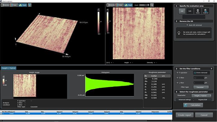
Measurement image showing planar roughness data