Background
The growing demand for small, high-speed mobile electronic devices with versatile features has caused a corresponding increase in the demand for high-density electronic components built on printed boards. This demand changed the way high-density components are made. Previously, integrated circuit (IC) components were manufactured using surface mount techniques, such as quad flat package (QFP) and small outline package (SOP). Increasingly, these components are produced using chip-on-board (COB) techniques where IC chips are mounted directly onto printed circuit boards. One popular method that is well-suited to manufacturing high-density components is a ball grid array technique called ‘flip chip,’ where bumps formed on a chip are connected directly to a printed board. This interface must be inspected to ensure that the connections are secure.
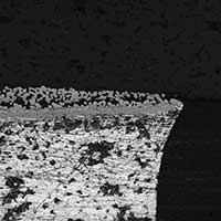
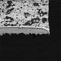
To analyze the interface, the chip is cut so that the connections can be directly observed using an optical microscope. However, the cut chip is polished before it can be viewed, and this process introduces fine surface irregularities which can make observation difficult. When this happens, manufacturers typically rely on an expensive electron microscope to make their inspections. The Olympus LEXT provides a fast and cost-effective solution to BGA inspection without the use of an electron microscope.
The Olympus solutions
The Olympus LEXT 3D measuring laser microscope features extended focal imaging (EFI), which uses the fine focus adjustment to combine many in-focus images from along the Z-axis. This results in an image of the entire field of view in focus. The LEXT has a minimum resolution of 0.12 μm. Using the LEXT, you will acquire clear images of surfaces containing fine irregularities that are similar to those you could obtain by using an electron microscope. In addition, the LEXT is capable of multicolor observations.
Features of the product
The Olympus LEXT features ultra-high-resolution combined with high pixel density (Figure 1). The EFI function enables you to bring the entire field of view into focus for easy inspection. The LEXT employs a variety of microscopy and image processing techniques that gives you the ability to highlight a feature point on the object being observed and make accurate measurements.
Image
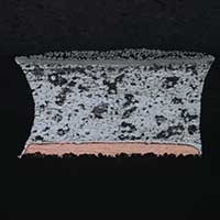 |  |  |
| Figure 1: A high-resolution image taken using the LEXT | ||