Microscope Solutions for
Semiconductor Manufacturing
Explore Microscope Solutions
for the Semiconductor Production Process
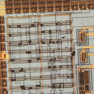 IC DesignIntegrated circuit (IC) design companies need to inspect the pattern of IC chips. Additionally, IC chip manufacturers must analyze the IC chip design at the trial production step. Since the inspection volume is low, manufacturers can use manual equipment with high accuracy. Our DSX1000 digital microscope is an easy-to-use system that can observe sub-micrometer patterns. | 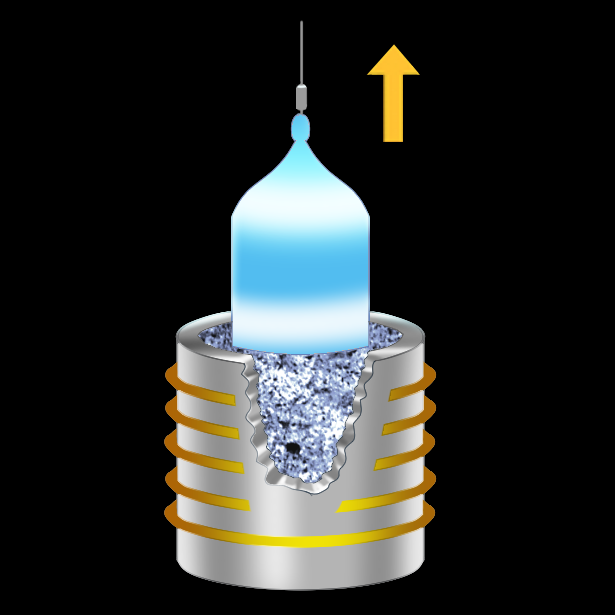 Making an IngotThe method for producing semiconductor wafers is the same regardless of the semiconductor materials: dissolve the materials into a mold to create a solid cylinder shape. The solid silicon is called an ingot. | 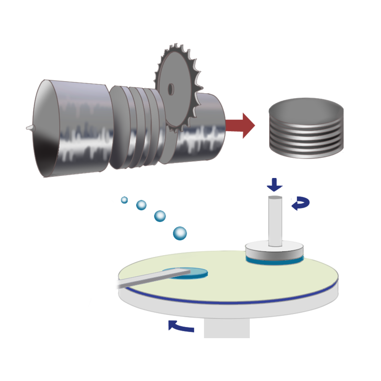 Slicing and PolishingSlice the ingot into thin silicon plates (wafers). Polish the top and bottom of the wafer surfaces. This flattens the surface so the circuit patterns can be imprinted. The polished wafer is then marked with laser marking equipment. Our OLS5000 laser confocal microscope can analyze surface roughness conditions after polishing. |
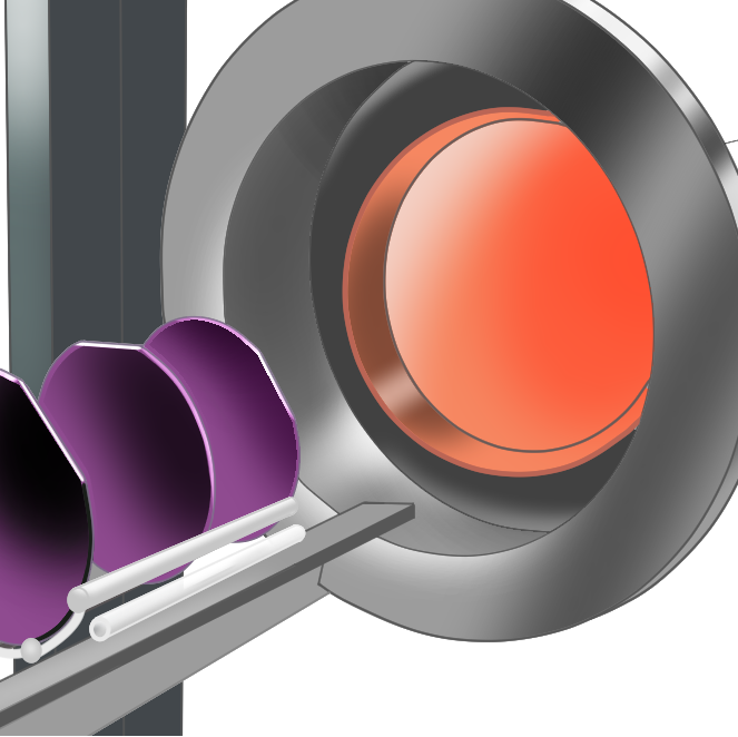 Oxidation on the Wafer SurfaceForm an oxide film on the wafer in a high-temperature oven. | 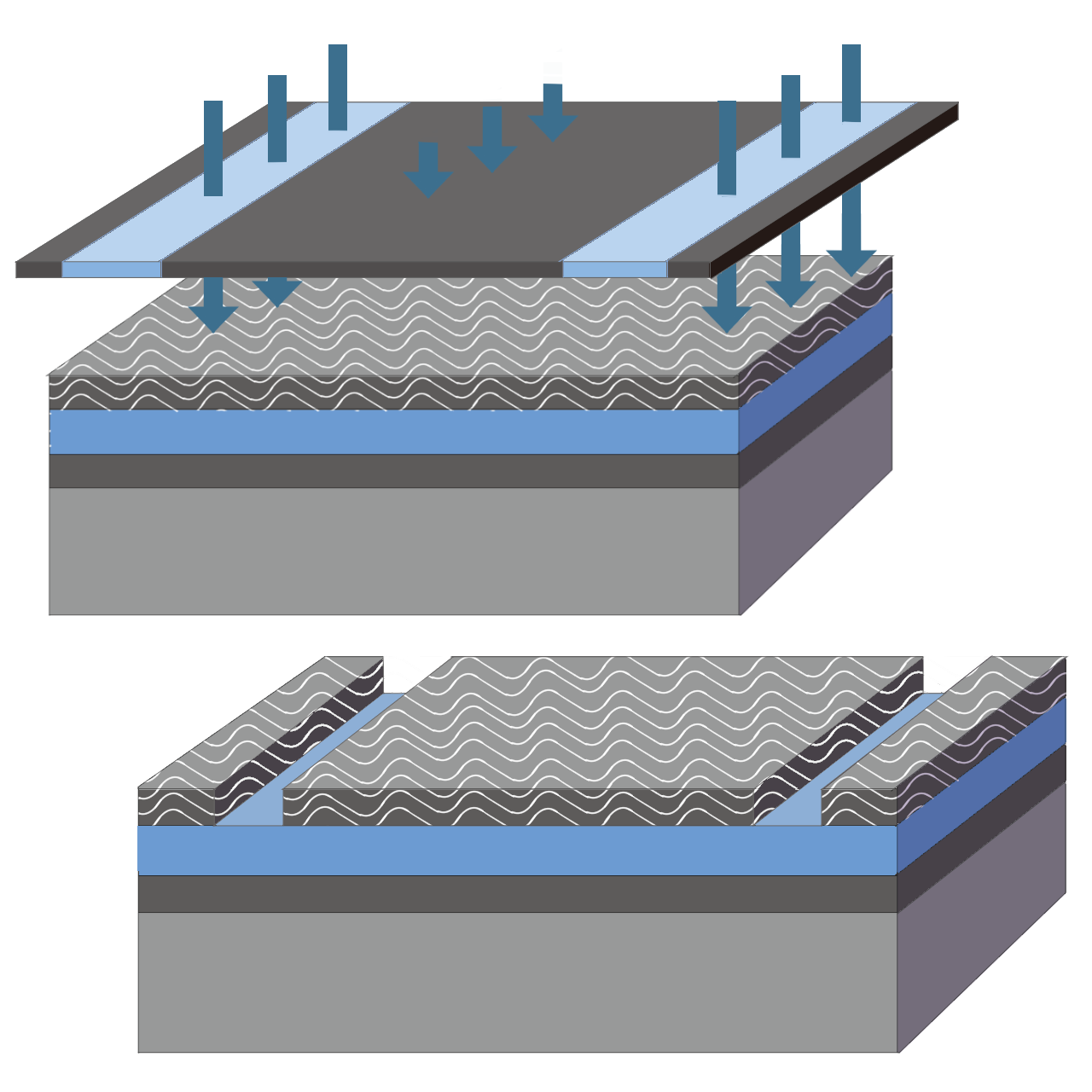 PhotolithographyPhotolithography is the process of imprinting integrated circuit patterns on the wafer. This process is repeated several times to make complex circuit patterns. Our OLS5000 laser confocal microscope can measure the thickness of the photoresist and pattern. | 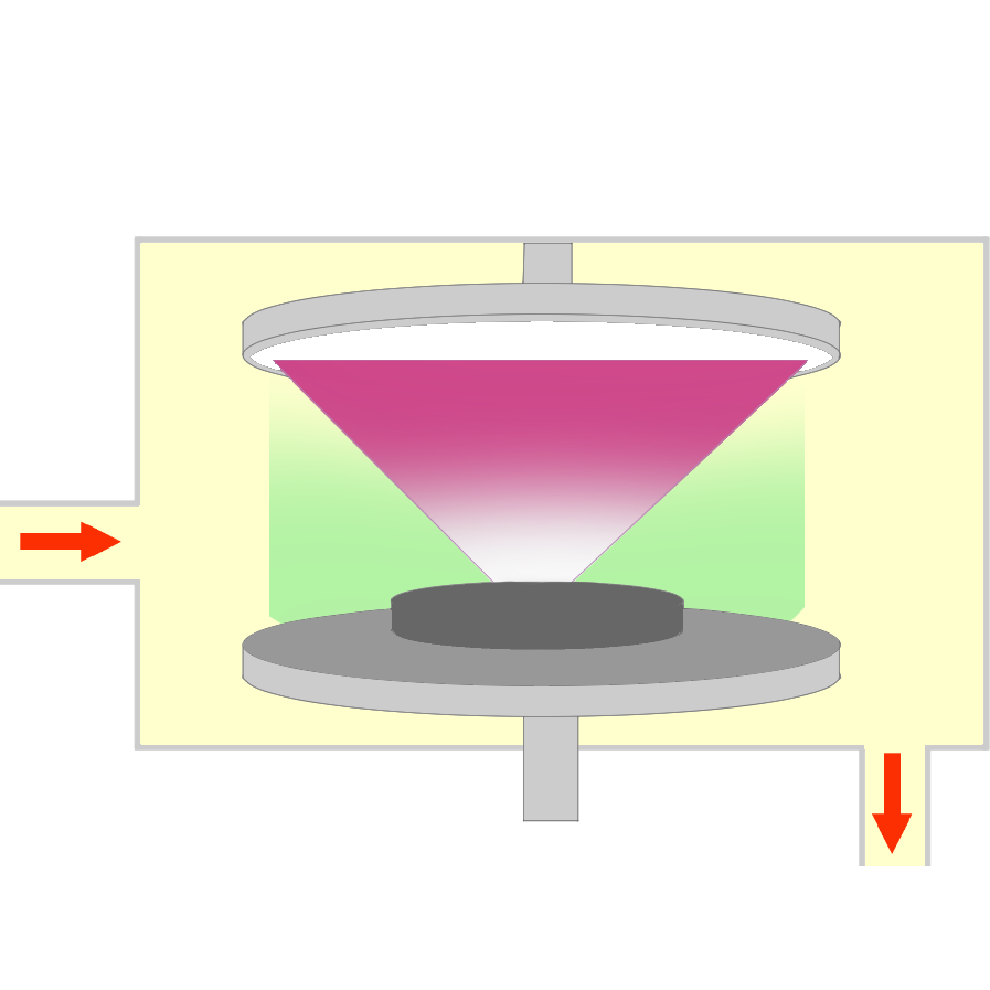 Making the Metal LayerInject ion beams to change the wafer material characteristics and deposit a metal layer to pass electric currents. |
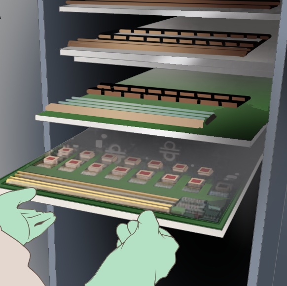
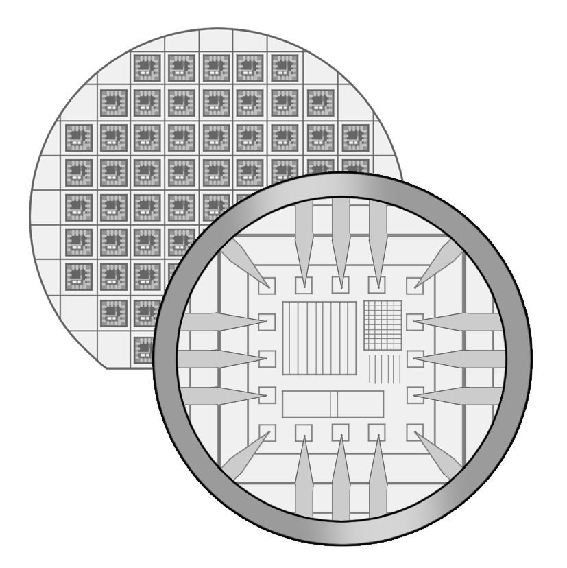 Electrical TestCheck if the wafer runs correctly with an electronics tester called a prober. Our DSX1000 digital microscope can quickly capture 3D images of the probe mark. | 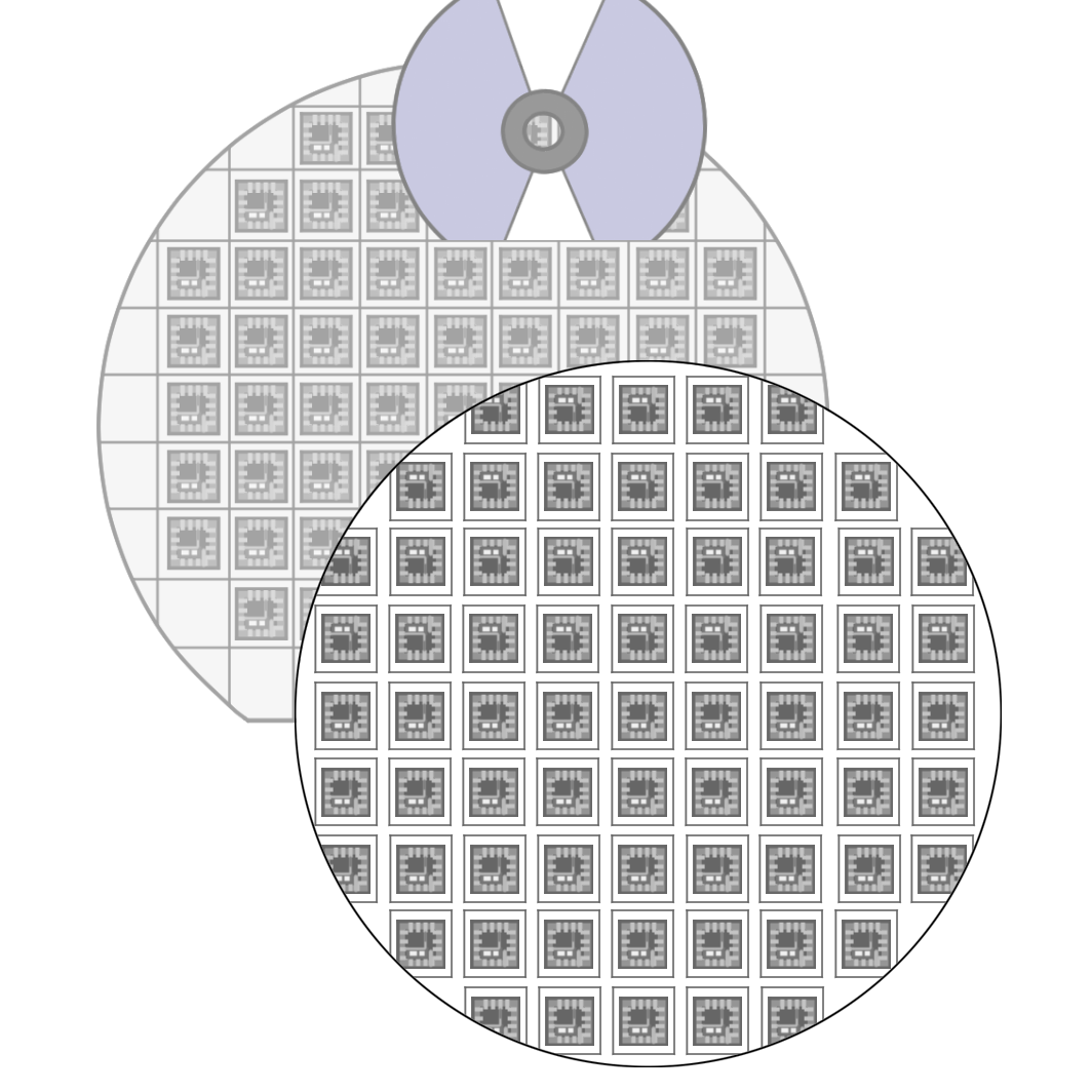 DicingA high-speed rotating blade cuts the wafer into individual chips. Our OLS5000 laser confocal microscope helps you check the chip size. | 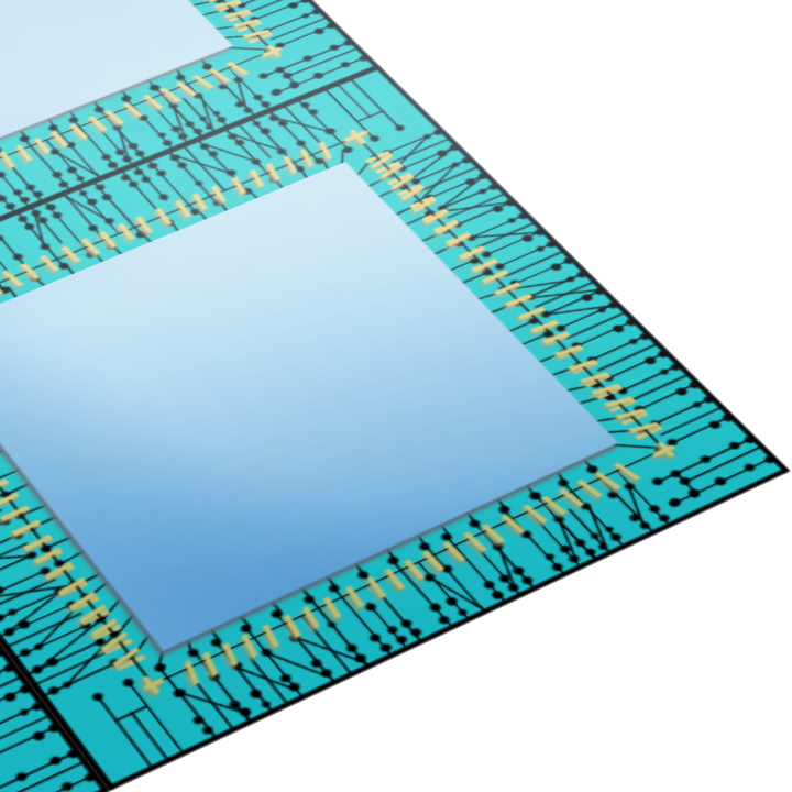 Die BondingMount the IC chips onto designated locations on load frames. Our BX and MX series industrial microscopes help you inspect and analyze defects after die bonding. |
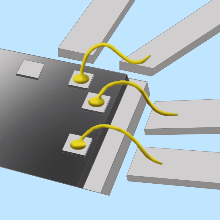 Wire BondingAn IC chip connects to external devices with wire bonding. Wire bonding is a method to weld between an IC chip and the lead frames. A wire is attached to a lead frame and an IC chip's aluminum pad using a combination of downward pressure, ultrasonic energy, and heat to make a weld. We provide a variety of solutions for lead frames, bonding wire, mashed balls, and other applications. | 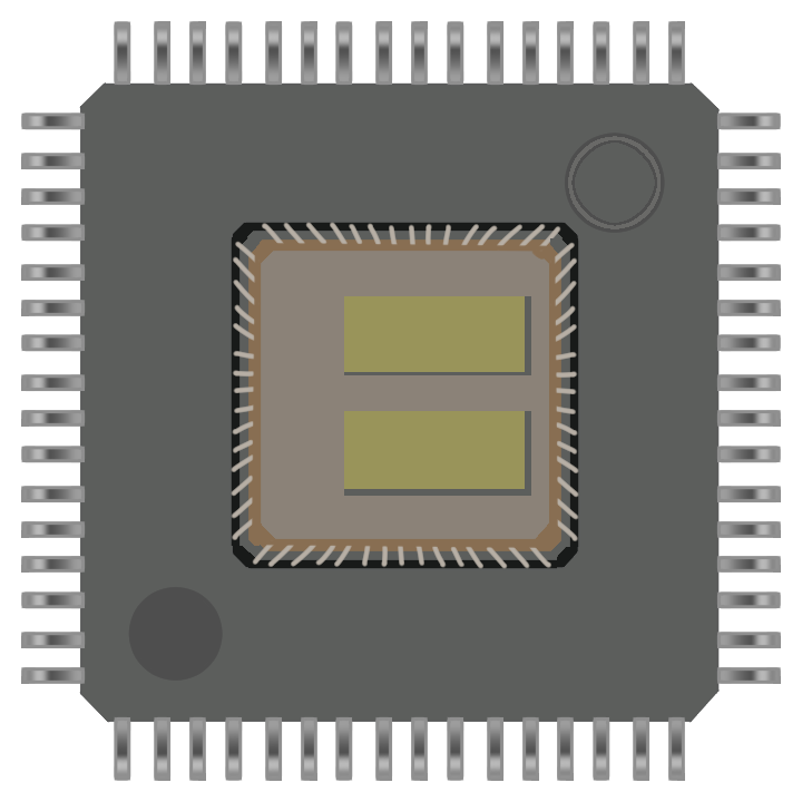 PackagingPackage IC chips using epoxy resin. Our SZ series microscopes can image the entire sample to check the appearance of the packaging. | 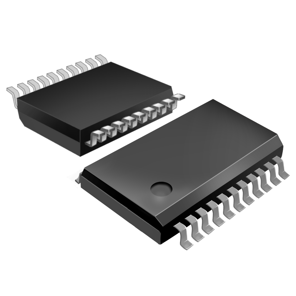 Cut the Lead FrameCut lead frames to separate the IC chip from them. |
 TestingConduct reliability tests and inspect the electrical characteristics/appearance to detect defects on semiconductors. | 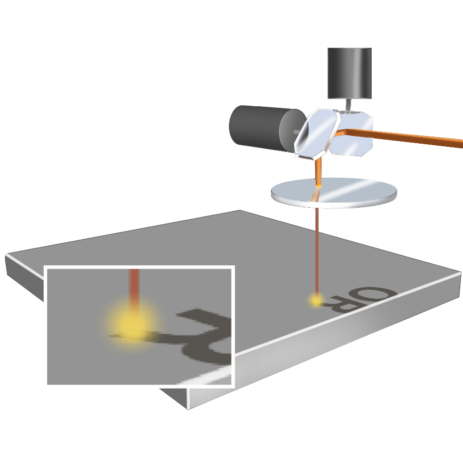 Laser MarkingPrint a product name on the IC package using laser marking. Our DSX1000 digital microscope is an easy-to-use system that provides clear images of laser markings. |