Microscope Solutions for
PCB Manufacturing
Explore Microscope Solutions
for the PCB Production Process
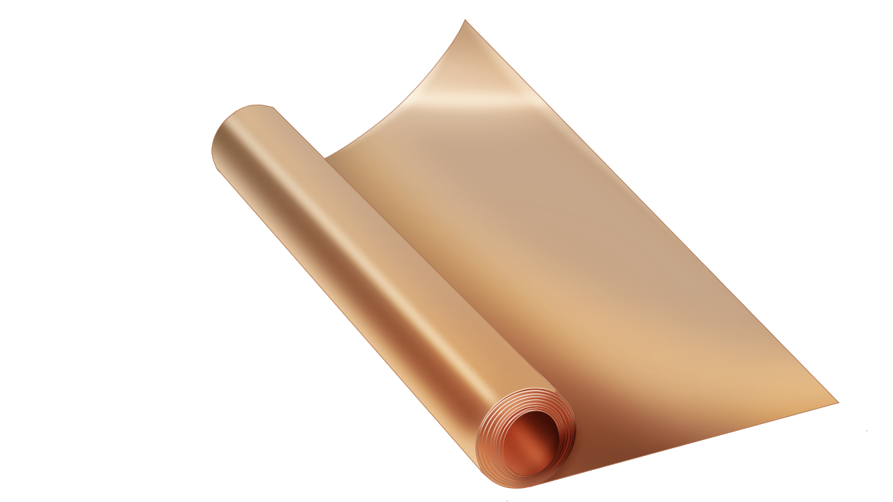 Making the SubstrateMake a substrate using glass and epoxy, then cover it with copper foil. The surface roughness of the copper foil must be carefully inspected because it influences the quality of the printed circuit board (PCB). Our OLS5000 laser confocal microscope can precisely measure the surface roughness of copper foil. | 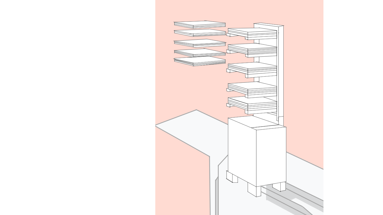 Making the Inner LayerAfter applying a resist to the copper foil, the surface is etched to form a circuit. This process is repeated many times to complete the inner layer board where the circuit is formed. Our DSX1000 digital microscope can quickly capture 3D image dimensions of the inner layer. | 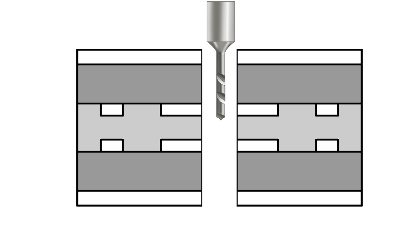 Drilling HolesDrill the PCB surface to create holes. These are known as through holes. Our BX series metallurgical microscope can detect smear caused from the drilling process with fluorescence observation. |
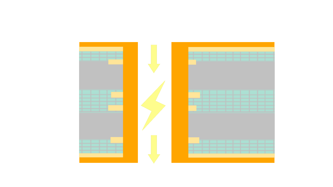 Processing the Outer LayerCircuits are formed on both sides of the multilayer substrate using the same process as the inner layer. Our DSX1000 digital microscope supports quality checks of through holes, via holes, copper patterns, and more. | 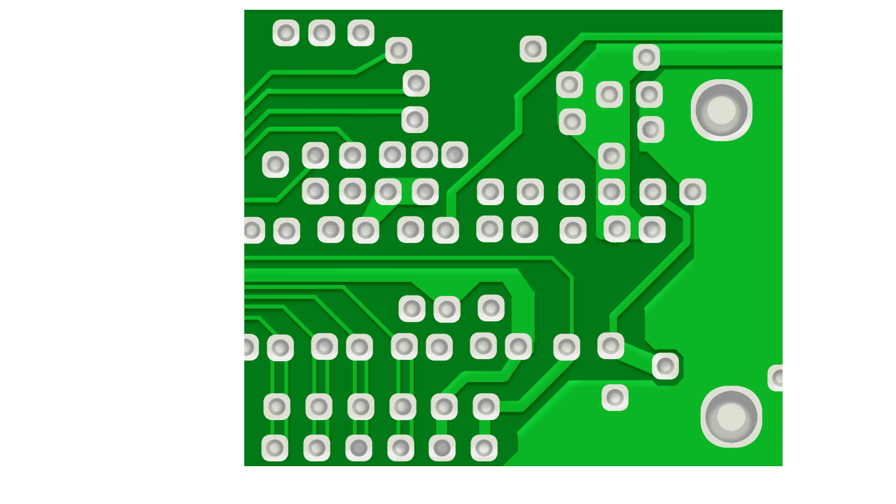 Placing the Solder ResistCover the PCB surface with a material called solder resist while avoiding any areas where electric parts will be mounted. | 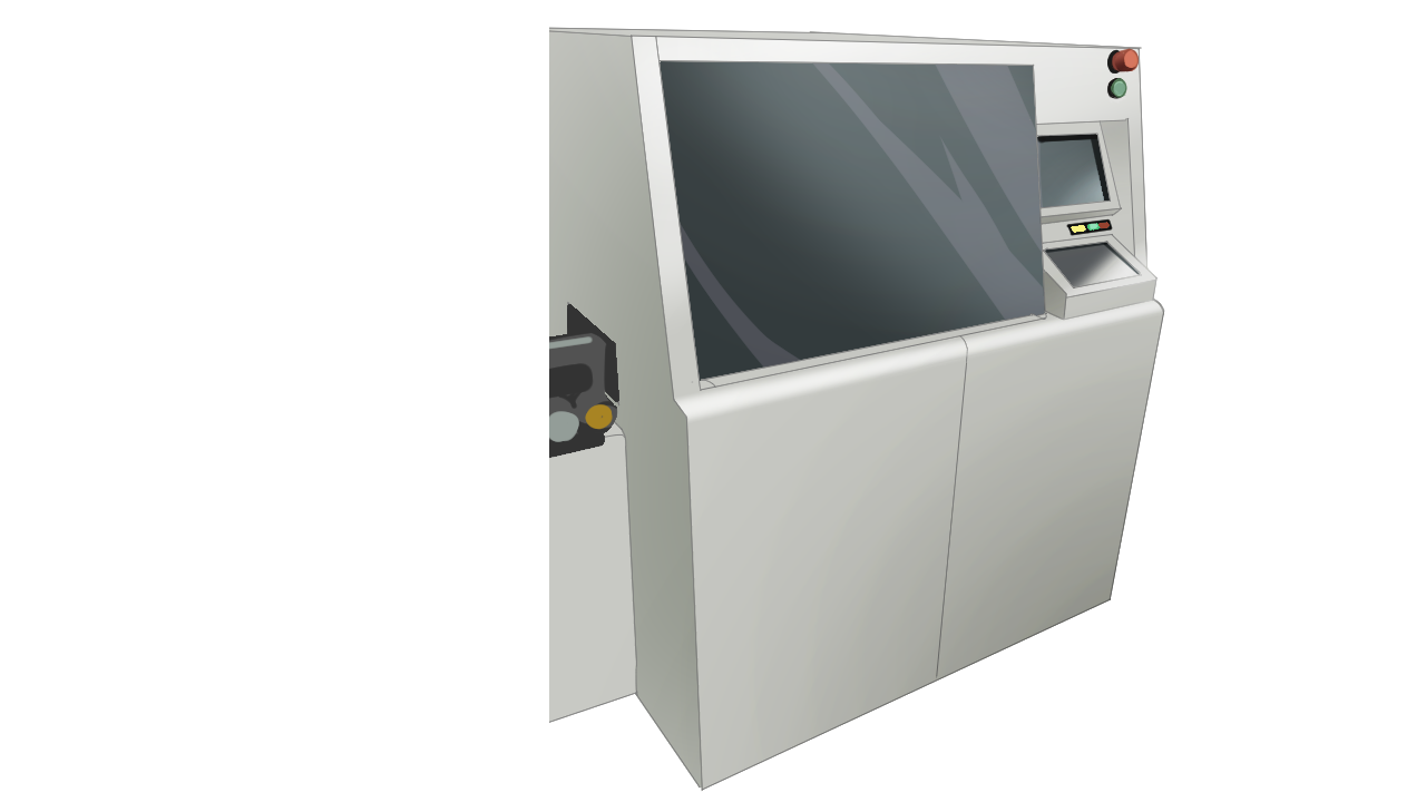 Pasting the Solder on the PCBPaste the solder on the PCB surface with a solder paste machine. Solder is a metal used to adhere electronics parts onto a PCB. Our BX series metallurgical microscope can observe the residues of flux that sometimes remain after soldering. |
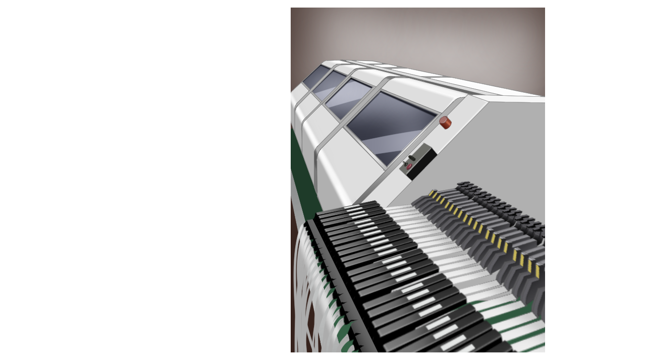 Mounting Electronics Parts on the SurfaceMount the electronics parts on the PCB with a surface mounting machine. To do so, heat the PCB using a heating machine to melt solder on the PCB. The melted solder adheres the electronic parts onto the PCB. Our DSX1000 digital microscope provides free-angle observation and quickly captures 3D images, enabling you to observe the quality of surface mounting, whiskers, and other components. |
