Semiconductor Wafer & Flat Panel Display Inspection Microscopes
Evident semiconductor wafer and flat panel display inspection microscopes provide the highest level of efficiency, ensuring fast start-up times, easy operation, failure analysis, and expandability for users. Our selection of semiconductor inspection microscopes is designed for the safe transfer of wafers, ideal for semiconductor defect inspection. In addition to automated wafer handling systems, a digital microscope may be employed for detailed analysis of small defects within semiconductors. Explore our complete range of flat panel display and semiconductor inspection microscopes below. |
Semiconductor Wafer Inspection Microscope
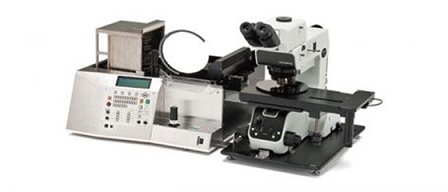
AL120
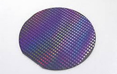
The AL120 wafer handler series is a semiconductor inspection microscope that enables the easy transfer of both silicon and compound semiconductor wafers, including silicon carbide (SiC) and gallium arsenide (GaAs), from the cassette to the microscope stage with enhanced capabilities and flexibility, all while maintaining an ergonomic, user-friendly design.
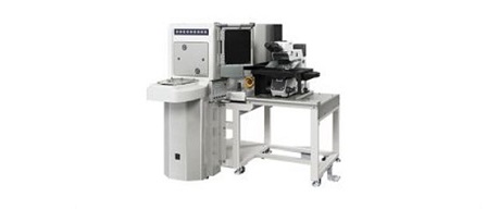
AL120-12
Ideal for lower-cost back-end inspection, the AL120-12 wafer handler is a semiconductor inspection microscope compatible with both FOUP (front opening unified pod) and FOSB (front opening shipping box). The safe and ergonomic design maintains operator safety while effectively transferring wafers, including thin and warped wafers.
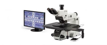
MX63 / MX63L
The MX63 and MX63L microscope systems are optimized for high-quality inspections of wafers as large as 300 mm. Compatible with flat panel displays, circuit boards, and other large samples, their modular designs enable you to choose the components you need to tailor the system to your application.
Semiconductor & Flat Panel Display Inspection Equipment
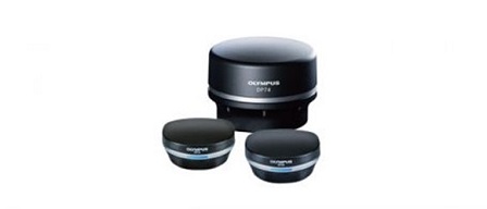
Digital Cameras for Microscopes
Evident digital microscope cameras enables you to capture high-quality images of samples. Featuring high resolution and excellent color fidelity our cameras enable crisp, live images to be displayed at full resolution, offering clear observation and real-time focusing.
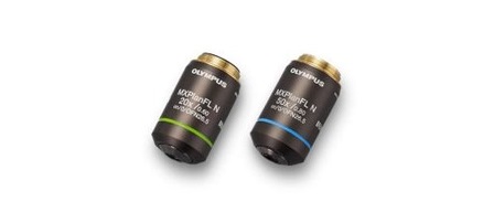
Semiconductor Wafer Inspection Objectives
Evident’s MXPLFLN Objectives Series was designed to deliver high resolution and long working distance simultaneously, ideal for semiconductor wafer inspection.
Additional Semiconductor Wafer Inspection Resources
Optimize Your Wafer Inspection Microscope and WorkflowLearn how semiconductor wafer manufacturers can improve wafer inspection quality control by optimizing their equipment and workflows. | 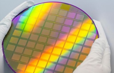 |
Capabilities of Near-Infrared Imaging for Electronics and Semiconductor InspectionDiscover how Evident inspection microscopes enhance near-infrared imaging for semiconductor inspection. | |
Circuit Pattern Inspection on Wafer SamplesDiscover how Evident’s MX63/MX63L industrial microscopes for semiconductor/FPD inspection provide an efficient alternative to conventional observation methods of wafer samples. |
|